What is data center CWDM4 transmission technology?
June 9, 2023
1、Data Center Optical Transmission Evolution of technology
With the promotion and application of mobile Internet, data centers are developing rapidly and have become essential infrastructure in the information society. Data centers consist of a large number of servers, which require high-speed, high-capacity data transmission and exchange among the servers. Traditional cable-based transmission methods are unable to meet the rate requirements. Since 2010, fiber optic transmission technology has entered the data centers and has become the mainstream transmission technology.
In the early stages, data centers were not large in scale, the required transmission distances were typically in the range of tens to hundreds of meters. They commonly employed multi-mode fiber parallel transmission technology and continuously optimized the dispersion performance of multi-mode fiber to support higher speeds and longer transmission distances. OM4-compliant multi-mode fiber can support the transmission of 10G signals up to 550 meters.
However, the mainstream transmission rate of data center has entered the 100G era, usually using 4×25G single-mode fiber. Multi-mode fiber is no longer able to support such high transmission rates, leading to the introduction of single-mode fiber in 100G transmission systems. In fact, the cost of single-mode fiber is higher than that of multi-mode fiber. However, single-mode fiber operates at a transmission wavelength 1310nm, while multi-mode fiber operates at a transmission wavelength of 850nm. Optoelectronic components operating in the 1310nm band are much more expensive than those operating in the 850nm band.
For single-mode fiber optic transmission of 4×25G optical signals, the PSM4 scheme is commonly used, This scheme utilizes eight fibers to achieve bi-directional data transmission between a pair of transceiver modules. PSM4 transceivers require only one laser that is split into four paths, each going through a separate modulator. This configuration helps to reduce the cost of the light source. However, as the transmission distance increases, the cost of optical fiber also increases rapidly. Therefore, PSM4 transceivers are usually used in scenarios where the transmission distance is less than 500 meters.
For applications with transmission distance exceeding 500 meters, in order to save fiber cost, data centers have adopted CWDM technology from telecom networks, specifically the CWDM4 transmission scheme. By using a wavelength division multiplexer/demultiplexer, four wavelengths with 20nm spacing(1271nm, 1291nm, 1311nm, and 1331nm) are transmitted over a single fiber. This enables CWDM4 to support 4×25G signal transmission between two fiber transceiver modules. In the transmission distance range of 500 to 2000 meters , the CWDM4 solution offers cost advantages over the PSM4 scheme. CWDM4 can support 4×25G signal transmission and provides a cost advantage in the 500-2000 meter transmission distance range.
2、CWDM4 technology solution
The application of CWDM technology has achieved significant maturity in telecommunication networks, and the International Telecommunication Union (ITU) has defined 18 CWDM channels with a 20nm spacing in the 1271-1611nm wavelength band. In data communications, the CWDM4 standard uses four wavelengths that are closely aligned with the zero dispersion points of G652 single-mode fiber, specifically within the 1271-1331nm range.
The current mainstream form factor for 100G fiber optic transceiver modules in data centers is QSFP28, which integrates four semiconductor lasers, an array of optical detectors and their driver circuits, and passive CWDM4 components. In order to integrate the CWDM4 components into the QSFP28 module, the design needs to be as compact as possible, with more stringent size requirements than the CCWDM module (a compact CWDM module) used in telecom applications.
1) Z-block technology
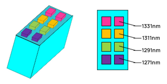
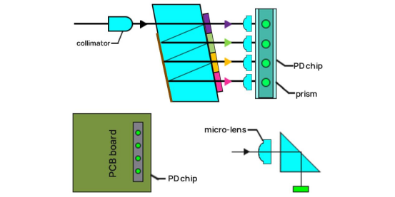
The earliest CWDM4 component was based on Z-block technology utilizing thin film filter(TFF). As shown in Figure 1, eight TFF filters affixed to a rhomboidal prism, divided into two groups – one for WDM and the other for WDM. Each filter is designed to transmit at specific wavelengths: 1271nm, 1291nm, 1311nm and 1331nm, respectively.
Figure 1. Z-block structure with CWDM4 filter attached
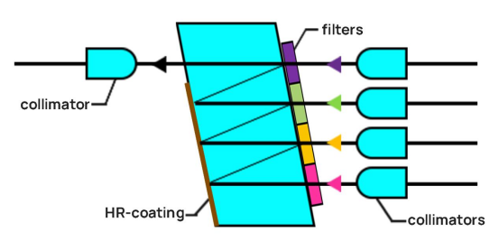
The WDM transmitting optical path of the Z-block assembly is shown in Figure 2. The rear part of the rhombohedral prism is coated with a highly reflective film. The optical signals emitted from the four collimators on the right side pass through the corresponding filters and are reflected at different times. They then reach the collimator at the common left end and are coupled to the output fiber. Due to the long optical path in the rhomboid prism, which is approximately 10 mm, a total of five collimators need to be used. The coupling of the reflected and collimated beams is highly sensitive to the angle, making it impractical to use an integrated array of collimators. Each input collimator must be independently adjusted for alignment, making the assembly process more complex.
Figure 2. Multiplexed transmitting optical path of Z-block
The Z-block assembly is shown in Fig. 3. The optical signal of the common terminal is input through the left collimator. the optical signal of each channel undergoes different reflection times, passes through the respective filter, and is focused onto the corresponding unit of the photodetector array by the microlens. The photodetector array is mounted on a PCB board, as illustrated in Figure 3(b). The light beam, which is multiplexed by wave decomposition in the horizontal plane, requires passing through a right-angle prism to make a 90-degree turn and then incident on the photodetector in the vertical direction. The size of the active area of the photodetector is usually only Φ50 µm, while the diameter of the collimated beam transmitted in the Z-block is much larger than this. This focusing process also increases the complexity of the Z-block assembly process.
Figure 3. Demultiplexed receive optical path of Z-block
2) AWG technology
In order to simplify the packaging process to reduce size and cost, the CWDM4 AWG chip based on integrated optical technology has been developed. AWG stands for Array Waveguide Grating, which has been widely used in telecommunication networks for a long time. AWGs are used in telecom networks for multiplexing/demultiplexing DWDM Optical signals. The channel spacing in these networks is usually 200G or 100G (corresponding to a wavelength spacing of 1.6nm or 0.8nm). Because these applications scenario is mainly the backbone of telecom networks, cost sensitive is relatively low.
The integration of AWG technology into the CWDM4 transmission system of data center has led to an increase in the wavelength spacing to 20nm, which has reduced the technical difficulties. However, in order to meet the size and cost constraints of QSFP28 modules and scale applications, the requirements for AWG chip size are much more stringent, the current mainstream CWDM4 AWG chips can be controlled within the size range of 2mm×10mm. The earliest CWDM4 AWG chips had input/output ports located at both ends, as shown in Figure 4. In order to facilitate fiber winding and integration into fiber optic transceiver modules, a single-sided input/output CWDM4 AWG chip was developed. This was achieved by bending the waveguide to connect the input port to the output port, as shown in Figure 5. This design also further simplifies the coupling process between the waveguide and the fiber array. Of course, due to the limited width of the chip, the bending radius of the waveguide is less than 1 mm, which introduces certain bending losses.
Figure 4. CWDM4 AWG chip structure – input/output on both sides
In a CWDM4 fiber optic transceiver module, two CWDM4 AWG chips are required, one for multiplexing the optical signal for transmitting and the other for demultiplexing the optical signal for receiving. The CWDM4 AWG chip at the transmitter side currently uses the single-side input/output structure shown in Figure 5, while at the receiver side, the demultiplexed wavelengths will eventually be detected by the optical detector and will not need to be coupled into the single-mode fiber for further transmission. For this reason, the CWDM4 AWG chip at the receiver side usually adopts the dual-side input/output structure shown in Figure 4. The output port utilizes a multi-mode optical waveguide and is equipped with a polished 45° bevel at the output side to achieve a 90-degree turn of the beam. This beam is incident on the photodetector array, which is mounted directly on the PCB board.
This design has two advantages. Firstly, the use of multi-mode optical waveguide output enables a flat design of AWG passband spectrum and optimize the channel quality. Secondly, the output light is directly injected into the photodetector array after a 90-degree turn, which eliminates the butt coupling between the waveguide array and the fiber array. This simplifies the assembly process.
3) Comb filter technology
Compared to Z-block technology, the CWDM4 AWG chip with integrated optical technology has a smaller size, and significantly simplified assembly process, which helps reduce costs. However, AWG devices suffer from poor passband flatness, degraded the channel quality, and much higher loss compared to Z-block technology.
Some vendors have introduced the optical comb filter ITL (Interleaved Tunable Laser) technology in telecommunication networks into the field of data communication. Figure 6 shows the optical comb filter based on integrated optical technology, which is composed of several cascaded MZI (Mach-Zehnder Interferometer) interference arms. In fact, the optical comb filter in telecommunication network is primarily used for DWDM applications, considering the temperature stability, usually using GTI resonant cavity or birefringent crystal schemes. Integrated optical comb filter are unable to meet practical requirements.
Figure 6. Optical comb filter based on integrated optical technology
However, the channel spacing of the CWDM4 transmission system is 20nm, and has a larger tolerance for temperature drift, so an integrated optical comb filter can be used. It should be noted that in Figure 6, the MZI interferometric arms achieve the optical range difference by bending the waveguide, which generates losses when the waveguide is bent. The minimum bending radius of the optical waveguide to avoid bending losses depends on the refractive index difference of the waveguide. To reduce the bending radius and chip size, existing suppliers are using silicon nitride waveguides. However, the larger the refractive index difference of the optical waveguide, the higher the yield will be affected, and the coupling loss with the fiber will increase.
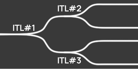
Optical comb filter is a 1×2 port device, in order to realize 1×4 WDM/demultiplexing, three comb filters need to be connected in series and parallel, as shown in Figure 7, where the wavelength interval of ITL#1 is 20nm, and the wavelength interval of ITL#2 and ITL#3 is 40nm.
Figure 7. CWDM4 chip consisting of three optical comb filters ITL connected in series and parallel
Both the optical comb filter and the AWG in CWDM4 system use integrated optical technology. The optical comb filter exhibits lower loss and better channel quality compared to the AWG, albeit with a slightly reduced yield.
3.CWDM4 technology comparison
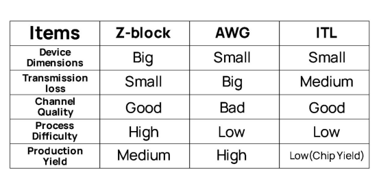
The advantages and disadvantages of Z-block, AWG and ITL CWDM technology solutions are shown in Table 1.
In comparison, Z-block technology has the advantages of low loss and good channel quality, and the CWDM4 module based on Z-block technology can even support 100G signal transmission for 10 km. However, this technology faces challenges in terms process complexity, resulting in high costs. The current problem lies in the low chip yield, but if this problem is solved, it will become the best solution for CWDM4.