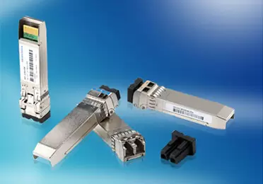
Optical modules are key transmission components in communication networks, and their applications, technologies, types, and terminology are diverse. It can be confusing for those new to the field. When discussing optical modules, what are we actually talking about?
This article aims to delve into the highly market-driven terminology form multiple perspectives. Starting from the inception of customer demands, it progressively covers the procurement of components, selection of technological paths, determination of packaging processes, and ultimately, the complete manufacturing process of optical modules. This is intended to offer readers a clearer overall understanding of optical modules.
The end-to-end process from demand to the completion of optical module design.
This article descibes the end-to-end manufacturing process of optical modules, starting from customer demands and proceeding through material selection, design, and production. The article systematically analyzes numerous terms, technologies, and categories within the optical module field. At the same time, it also briefly introducing industry development trends.
Requirements analysis
Using the data center as an example, the customer requirements is a transmission distance of 500 meters at a speed of 100G, utilizing a QSFP28 interface, while also considering the overall system cost. This concise requirement encompasses every key detail in optical module design and manufacturing.
Selection 1: Packaging Method and Process Route. We can choose between hermetic packaging options such as TO-CAN, BOX, and butterfly, or non-hermetic packaging options like COB, COC, etc.
Selection 2:Types of optical module. The various types such as VCSEL, DFB, EML, or narrow linewidth tunable can be choose.
Selection 3: Design Route. It can be a single-channel or multi-channel design.
Selection 4: Modulation Format. It can be NZR, PAM4, Coherent Modulation (such as QPSK, 16QAM, 64QAM, etc.)
Selection 5: Future development. Considering the continuously increasing data rates, outsourcing optical engines, and emerging technologies like silicon photonics.
These choices are directly related to several key performance indicators required by the product, and they are closely linked to the overall reliability and cost of the final product. In the competitive field of optical modules, it’s necessary to find the optimal balance among a combination of parameters.
This involves pursing performance aspects such as data rates, small form factors, and long transmission distances. It also entails addressing power consumption and thermal management challenges. Addressing thermal management concerns may, in turn, raise cost considerations. Managing costs, in turn, involves risks related to stability and reliability, among other factors.
Therefore, despite the standardization of packaging, appearance, and electrical interfaces, the design and manufacturing of optical modules still require extensive experience. Understanding customer requirements and striking a balance between performance, power consumption, cost, and reliability are the essence of a company’s core competitiveness in the optical module industry.
In this challenging process, designers need to navigate various technical and business considerations while maintaining optimal performance. They need to ensure that the product remains competitive in the market with outstanding performance.
The Selection of Form Factor
Hermetic Packging
Based on customer requirements and the outdoor environments, where laser chips are susceptible to vapor corrosion and temperature fluctuations that can significantly affect wavelength, we are considering adopting a hermetic sealing solution. This solution involves sealing the laser chip within a metal enclosure, filling the enclosure with inert gas, and including a sealed window for laser transmission. Depending on factors such as transmission distance, chip heat generation, cost requirements, and the number of channels, we can choose different hermetic sealing methods.
(1) TO-CAN Package
The laser diode is placed on a small heat sink (heat spreader) and connected via wire bonds to electrical pins. Subsequently, a metal cap is sealed on to the laser diode, including a sealed window for laser transmission. TO-CAN packaging offers a compact size and relatively low cost, making it suitable for applications in the telecommunications market, such as 10km 10G/25G transmission in areas like base station front-haul and home broadband.
However, due to its small size, it may not be well-suited for high-power, high-current, and long-distance transmission scenarios. This is because it is challenging to incorporate larger heat dissipation devices into such compact designs.
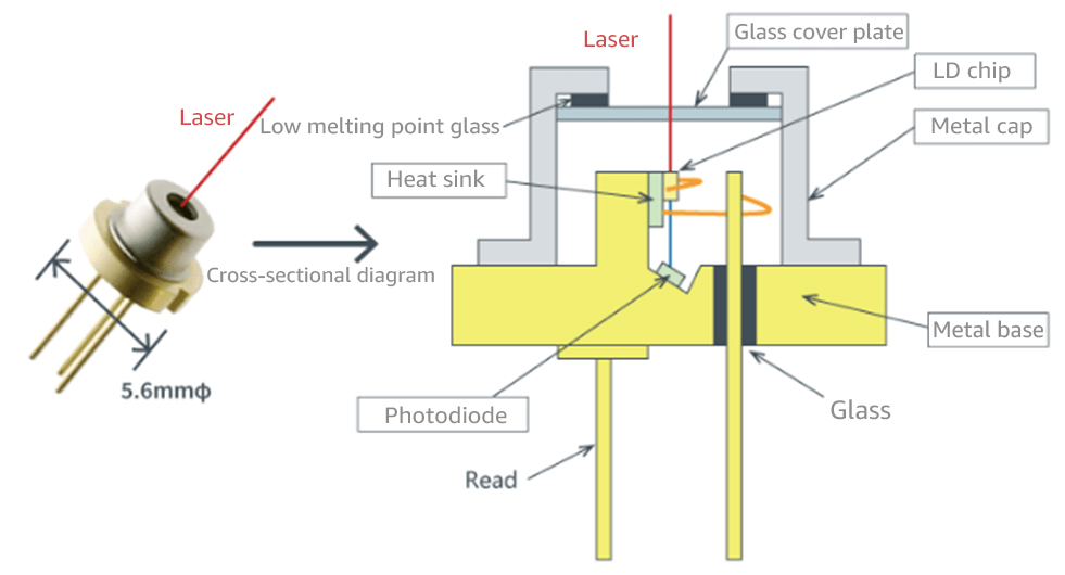
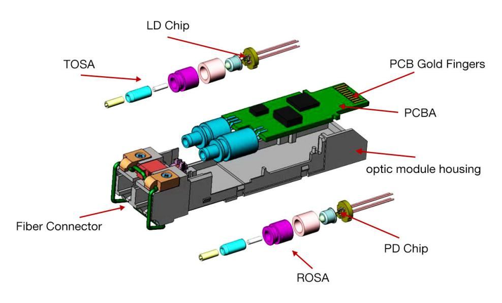
After being assembled into a TO-CAN, it essentially provides the basic packaging for the laser diode. However, the laser beam’s diameter may still differ from that of the optical fiber. Further alignment and coupling with lenses and optical fibers are required to focus the majority of the energy into the optical fiber.
Once all the components are fully packaged, it becomes a TOSA (Transmitter Optical Subassembly). On the other end, when using a receiver chip, it is referred to as a ROSA (Receiver Optical Subassembly). Collectively, these are known as OSA (Optical Subassemblies).
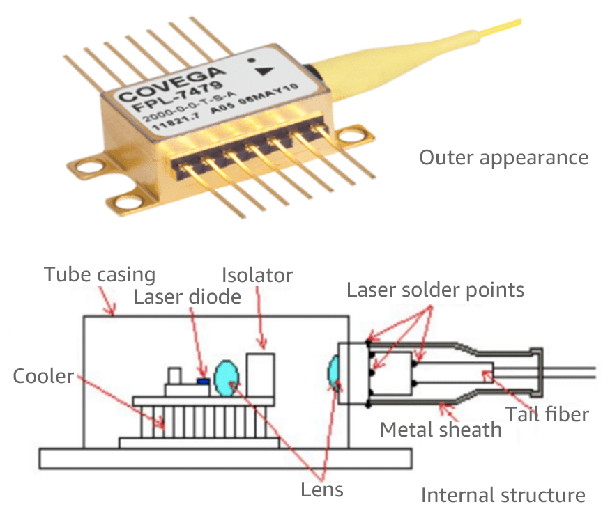
(2) Butterfly Package
To meet high-power requirements, a butterfly packaging solution can be employed. The laser diode is mounted on a larger heat sink, and a TEC (Thermoelectric Cooler) temperature control system can also be optionally used. Optical components such as lenses and isolators are also housed within the metal enclosure.
(3) BOX Package:
The BOX package is a specialized form of butterfly packaging designed to meet multi-channel requirements. Inside the BOX package, multiple laser diodes are integrated, and they are transmitted through a single optical fiber. This type of packaging is suitable for applications that have higher demands for temperature control, hermetic sealing, and reliability. Multi-channel issues will be discussed in more detail later, but they are briefly mentioned here.
Non-hermetic Packaging
As optical modules are widely utilized in the market, data centers have equipped themselves with air conditioning and environmental monitoring devices. Compared to the outdoor telecommunications market, data centers offer a more optimized working environment. This widespread use of optical modules has placed higher demands on cost control, leading to the gradual emergence of non-hermetic packaging technologies. This technology continues to evolve, with a continuous improvement in reliability, and its applicable scenarios are also expanding.
Non-hermetic packaging, in simple terms, involves directly attaching or soldering optical chips onto a printed circuit board (PCB) and using adhesive materials like epoxy resin for basic sealing. This approach reduces the need for many auxiliary components, thus improving cost-effectiveness and integration.
COB (Chip on Board) packaging is indeed a typical form of non-hermetic packaging. In COB packaging, components such as laser chips, laser arrays, and receiver arrays are directly attached or bonded onto a PCB (printed circuit board) substrate, achieving a compact form of packaging. This approach eliminates some protective measures and auxiliary devices, making it a relatively cost-effective choice.
For optical modules operating at 25Gbps and below, single-channel TO or butterfly-packaged optical transceivers components are typically soldered onto a PCB board. However, for high-speed optical modules operating at 40Gbps and above, there is often a need to use multiple channels in parallel due to limitations imposed by laser diode speed. For instance, 40Gbps can be achieved by aggregating four 10Gbps channels, and 100Gbps can be realized by combining four 25Gbps channels.
This places higher demands on packaging, including parallel optical design, managing high-speed electromagnetic interference, reducing physical size, and addressing heat dissipation issues, among others. COB packaging is a solution well-suited to meet these demands. It allows for the integration of TIA (Transimpedance Amplifier) / LA(Limiting Amplifier) chips, laser arrays, and receiver arrays into a compact package, enabling miniaturization of the module.
In summary, hermetic sealing provides a robust protective barrier constructed with metal and glass, making it suitable for various environmental conditions. However, non-hermetic packaging, when operating within controlled working environments, can optimize costs while meeting specific requirements.
Optical Chips Selection
When selecting optical chips, it is necessary to consider multiple factors comprehensively, including transmission distance, modulation methods, and cost. Additionally, the state of the supply chain is also an important consideration because certain popular products may experience shortages, delays, or delivery postponements during the early stages of production.
The semiconductor industry operates with significant economies of scale, and most chip manufacturers prioritize supplying large customers, while smaller manufacturers may need to seek alternative suppliers or solutions.
Due to differences in demand, there can be significant price variations when acquiring chips among optical module companies. Some larger companies with high demand may secure a price advantage of 20-30% lower than smaller manufacturers, making it a critical competitive factor in the optical module industry. Therefore, in the process of chip selection and procurement, supply chain and pricing factors also need to be carefully considered.
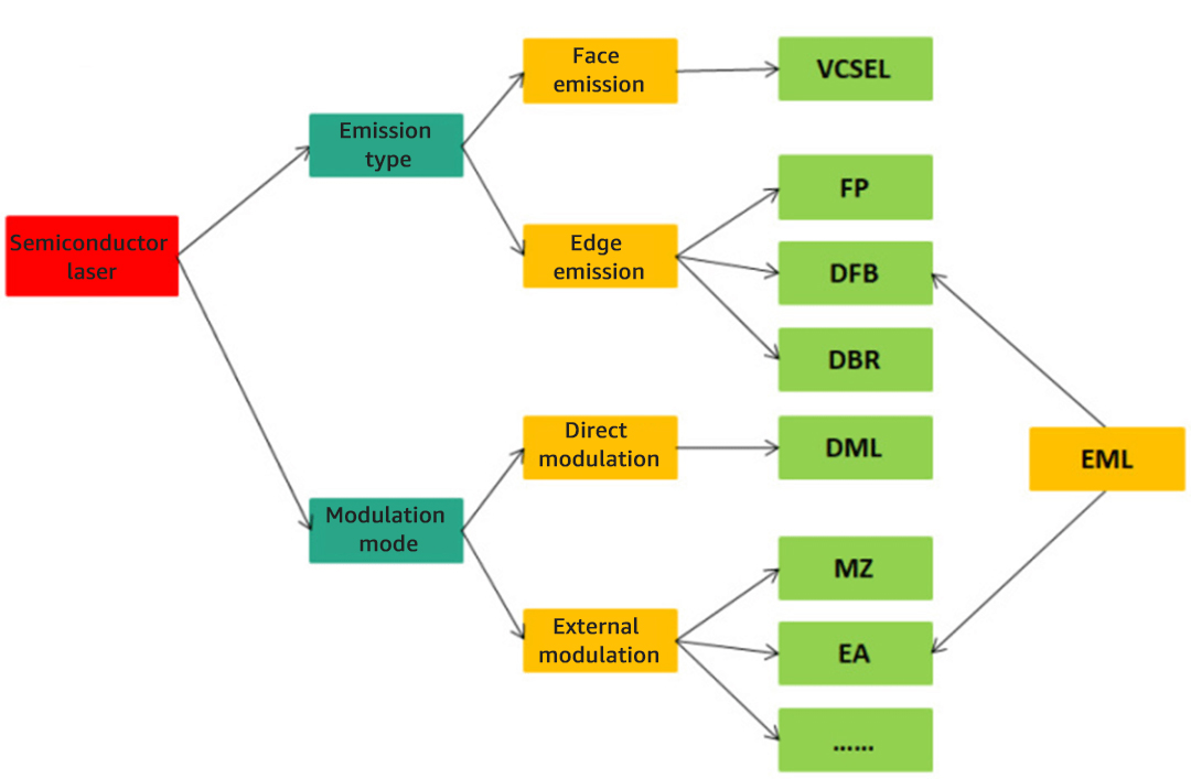
VCSEL Chip
VCSEL chips are a cost-effective choice with a larger emission angle, typically used in conjunction with multi-mode fibers. However, multi-mode fiber tends to be more expensive. When considering the overall system cost, it is more suitable for sort-distance applications, such as a few meters for AOC (Active Optical Cable) and approximately 100 meters for SR (Short-Range) optical modules.
DFB Chip
DFB (Distributed Feedback) chips are processed with gratings on top of the original FP (Fabry-Perot) laser to achieve more precise wavelength selection, thereby improving the accuracy of the output wavelength. The DFB chips have a narrower emission angle, enabling more efficient optical path coupling. As a result, DFB chips are more commonly used in medium to long-distance applications, such as 500 meters or 2 kilometers, and they offer a relatively moderate cost option.
EML Chip
EML (Electro-Absorption Modulated Laser) chips are a higher-cost option, consisting of a laser chip (which can be DFB, DBR, etc.) and an external electro-absorption modulator. During operation, the laser chip remains in a continuous emission state, and the signal output of the EML laser is controlled by toggling the state of the absorption chip. The advantage of using EML lies in the stable operation of the laser chip, resulting in a purer emitted wavelength. Even after modulation by the external modulator and long-distance transmission, the signal quality remains high.
EML is suitable for long-distance transmission applications, such as 10 kilometers, 20 kilometers, 40 kilometers, or even longer distances. However, due to the requirement for an external electro-absorption modulator and the higher quality demands associated with long-distance applications, the cost of EML chips is relatively higher than DFB chips, by as much as 50% or even more, at the same data rate.
Tunable Narrow-Linewidth Laser (Tunable Laser)
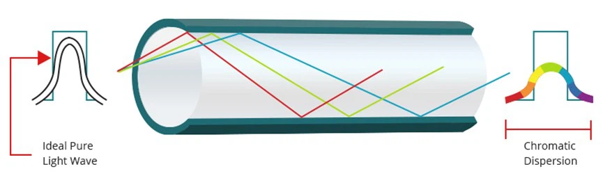
In the previous discussion, we mentioned that long-distance transmission encounters dispersion issues, and while EML (Electro-Absorption Modulated Laser) can address chirping-related problems, the inherent emission wavelength range of the laser, known as the ‘linewidth’, still persists. This issue remains prominent in ultra-long-distance ODN (Optical Distribution Network) applications, such as 80km, 100km, or even longer distances.
On the other hand, for ultra-long-distance trunkline transmission, the consideration of overall system cost is crucial. Laying a substantial amount of optical fiber from Beijing to Shanghai incurs significant expenses. Therefore, the introduction of DWDM (Dense Wavelength Division Multiplexing) technology, which enables the transmission of signals at different wavelengths over a single optical fiber, greatly enhances the transmission capacity of a single fibers and reduces the overall system cost for long-haul trunklines. Meeting these dual requirements necessitates the use of tunable narrow-linewidth lasers.
The structure of a tunable narrow linewidth laser is complex, and there are various approaches to achieve it, including current control, temperature control, mechanical control, and more. Taking the external cavity mechanical control approach as an example, a grating structure is added outside the ordinary laser, and the output wavelength is adjusted through mechanical control to achieve more precise wavelength control.
Tunable lasers have historically found limited applications, but with the potential introduction of wavelength division multiplexing (WDM) technology in 5G front-haul, some manufacturers are exploring the possibilities of using tunable lasers. The future demand for these technologies may undergo significant changes.
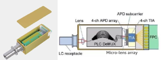
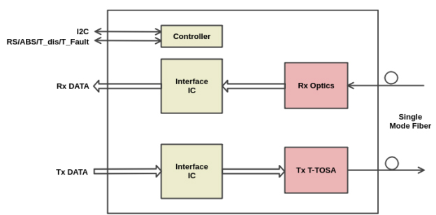
In this regard, Ascent Optics offers the Tunable SFP+/XFP 10G DWDM 80km Optical Transceiver Module to meet the current requirements of 5G front-haul WDM applications. Below is the schematic diagram of the module’s principle.
In conclusion, selecting the appropriate optical chip is crucial based on different transmission distances, modulation methods, and special requirements. VCSELs are suitable for low-cost short distances, DFB lasers are suitable for medium distances, EMLs are suitable for medium to long distances and special modulation needs, while tunable narrow linewidth lasers are suitable for ultra-long distances and special applications.
Selection of Design Routes
In the optical module design process, we have already chosen an appropriate packaging form based on the operating environment, and selected the suitable laser type according to the transmission distance and performance requirements. Next, we need to choose the number of channels and modulation method based on the transmission rate.
In the design process, we must navigate a delicate balance among several key metrics, including chip grade (performance and cost), number of channels (miniaturization, heat dissipation, packaging complexity), and modulation method (chip cost, reliability, design complexity). By conducting comprehensive assessments and trade-offs in these aspects, we will ultimately determine the optimal optical module design solution.
Single channel
The simplest solution. An optical module containing one laser and one receiver for single-channel transmission.
For example, a 10G chip can be used with NRZ modulation to create a 10G optical module. Or a 10G chip can be used with oversampling modulation to create a 25G forward error correction (FEC) optical module. And a 50G chip can be used with PAM4 modulation to create a 100G DR1 data center optical module. This type of design is suitable for single-channel requirements.
Multi-channel
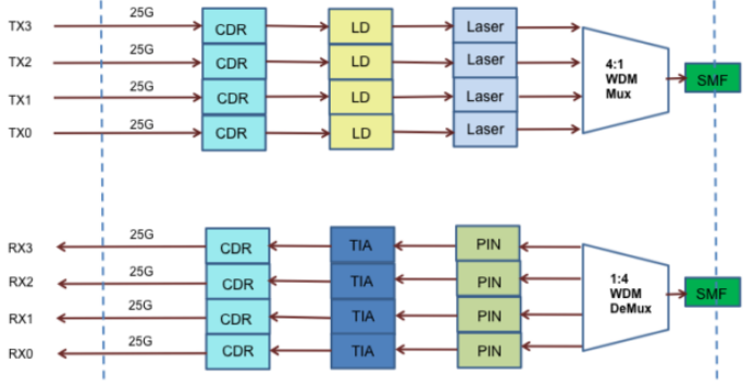
As customer demands for bandwidth increase, multi-channel design becomes one of the solutions. In this design multi-channel lasers and receivers are combined to achieve higher transmission rates. However, multi-channel design faces the challenge of how to transmit data over optical fibers effectively.
Multi-mode solution:
Each laser is directly connected to a single optical fiber for transmission. This design is simple, requires fewer components, and has relatively lower costs. However, when dealing with longer transmission distances, the multiple-fiber approach can exert significant cost pressure due to the cumulative cost of each optical fiber. This approach is suitable for medium to short-distance scenarios.
Single-fiber solution:
To reduce the amount of optical fiber used, a single-fiber solution can be employed. This approach utilizes the principle of Coarse Wavelength Division Multiplexing (CWDM), combing signals from four different lasers onto a single optical fiber for transmission and separating different wavelength signals at the receiving end for detection. The two main technological routes for achieving this are TFF (Thin Film Filter) filtering and AWG (Arrayed Waveguide Grating) devices.
TFF (Thin Film Filter) Filters:
This approach involves the use of filters to separate wavelength from different lasers before they enter the optical fiber. This method has relatively low temperature sensitivity but is associated with greater design and production complexity.
AWG (Arrayed Waveguide Grating) Devices:
Wavelengths are combined and separated using AWG chips. Although this method has relatively higher temperature sensitivity, it is associated with a relatively simpler design.
These two sub-solutions each have their characteristics. AWG devices are relatively temperature-sensitive and require higher temperature control capabilities, resulting in relatively higher costs (under similar yield and production volumes). However, the design and production phases are relatively simpler for AWG devices.
On the other hand, the TFF solution is less temperature-sensitive, but it involves greater difficulty in device design and manufacturing, requiring advanced skills in areas such as design, coating, and coupling alignment.
Selection of Modulation Format
When selecting the appropriate modulation format, it is important to consider the pros and cons of different approaches, and conduct a detailed comparison. Here are several common modulation format and their characteristics:
NRZ modulation
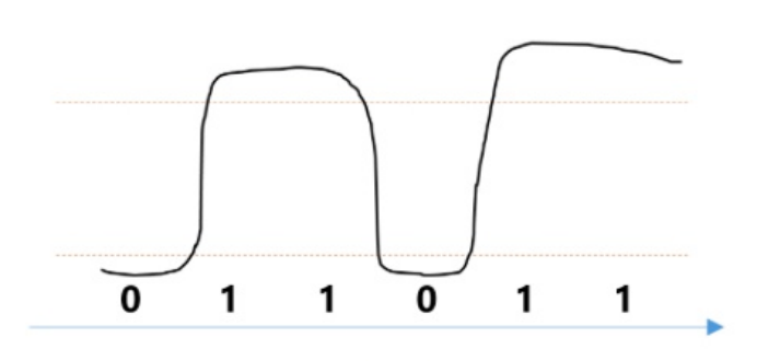
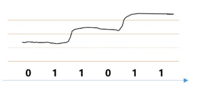
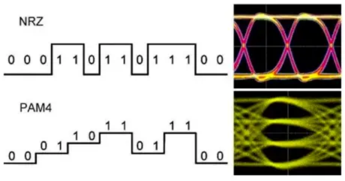
NRZ modulation is a traditional optical module modulation method, and its principle is relatively simple. Under NRZ modulation, the high/low optical power emitted by the laser corresponds to binary 1 and 0 signals, respectively. This modulation method is easy to understand but may have limitations for high-speed data transmission.
The required chip components are relatively simple, typically including a driver chip, amplifiers (TIA, LA), clock recovery circuit (CDR), and a control chip (MCU or ASIC). NRZ modulation is suitable for some short to medium-distance data transmission scenarios, such as connections within data centers.
PAM4 Modulation
To achieve higher data transmission rates, PAM4 modulation technology has been introduced. PAM4 modulation divides the optical signal’s power into four different thresholds, corresponding to the binary signal states 00, 01, 10, and 11. By employing a denser power level scheme, PAM4 can transmit more data in the same amount of time, thereby increasing the transmission speed.
Due to the precise power control and narrower detection thresholds required by PAM4 modulation, it typically necessitates the use of an External Cavity Laser (EML) laser diode. In addition to the chip components required for NRZ modulation, a Digital Signal Processor (DSP) chip is also needed for signal processing, converting digital signals into analog signals.
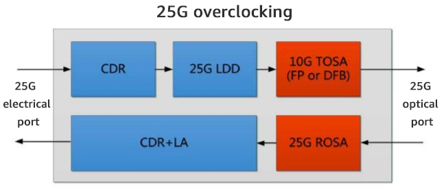
Overclocking Scheme
The overclocking scheme is used to reduce costs by using low-speed chips to transmit high-speed signals. For example, it is possible to use a 10Gbps optical chip to transmit a 25Gbps signal. However, this approach may lead to a decrease in signal quality because overclocked signals can encounter issues with reduced threshold recognition during the laser’s emission ramp-up process.
Currently, there are two common configurations for 25G optical modules: 25G optical chip-based modules and overclocking of 10G optical chips. Compared to overclocking 10G optical chips, 25G optical chip-based modules offer higher reliability and stability, even though they have more stringent production process requirements.
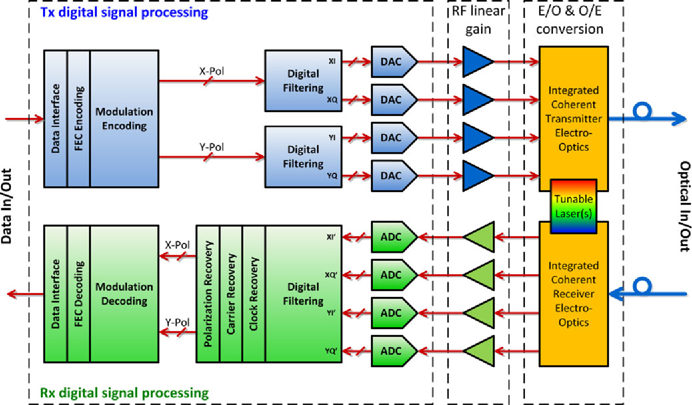
Coherent Modulation
Coherent modulation is a special modulation technique that utilizes both the phase and amplitude parameters of a signal. It offers two main advantages: Firstly, it can transmit more data within one signal cycle, similar to PAM4 modulation. Secondly, it achieves excellent interference immunity through techniques like differential phase-shift keying, making it suitable for ultra-long-distance transmission.
Coherent modulation technology indeed offers unique advantages for ultra-long-distance transmission. However, compared to traditional modulation methods, its implementation is more complex and requires more advanced modulation devices and algorithm support.
In conclusion, the choice of modulation method needs to take into account multiple factors, including transmission requirements, optical chip characteristics, and cost. Additionally, considerations should be given to standardization of form factors and interface to ensure compatibility and interoperability of optical modules. When designing optical modules, it’s essential to strike a balance between these various parameters and constraints to achieve the optimal design solution.
Summary
Through this comprehensive analysis in this article, we have gained an in-depth understanding of the design and applications of optical modules, covering multiple key aspects and technical considerations from source to endpoint. Optical modules, as a core component in the modern communication field, playing a crucial role in areas like data centers and cloud computing. They also demonstrate significant potential in emerging applications such as 5G communication and the Internet of Things (IoT). In the backdrop of such diversity and rapid development, we can offer some prospects for the future of optical modules.
As communication technology continues to advance, optical modules will continue to evolve towards higher speeds, smaller form factors, and greater reliability. From 10G, 25G to 100G, and 400G, the continuous increase in transmission rates will provide greater bandwidth and capacity for data transmission. Additionally, with the advent of the 5G era, the application of optical modules on wireless communication will continue to grow. For instance, in optical modules used for fronthaul and network connectivity. This will greatly accelerate the speed and intelligence of data transmission.
Furthermore, as the importance of sustainability continues to grow, optical module design will also place greater emphasis on energy efficiency and environmental considerations. In the design process, we will consider strategies such as reducing power consumption, improving heat dissipation efficiency, and using renewable materials.
In the future, with continued technological innovation and breakthroughs, optical modules will play an more critical role in driving advancements in the field of information and communication technology. Whether in data centers, communication networks, or emerging applications, optical modules will continue to evolve. They aim to provide people with faster and more reliable connections, making information transmission more convenient and efficient.
In conclusion, optical modules, as one of the key drivers of communication technology, have a future full of hope and challenges. We look forward to witnessing more innovative breakthroughs in this field, paving the way for a brighter future in global communication.
Post Views: 11,909