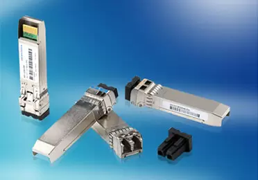
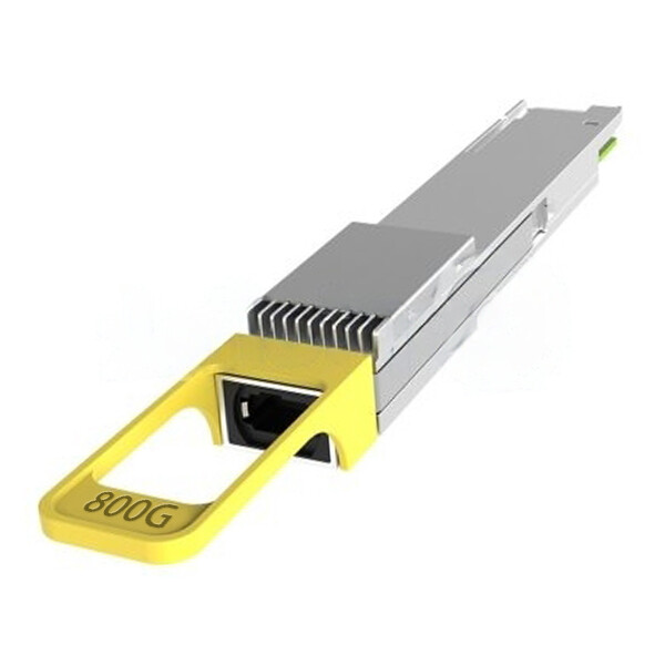
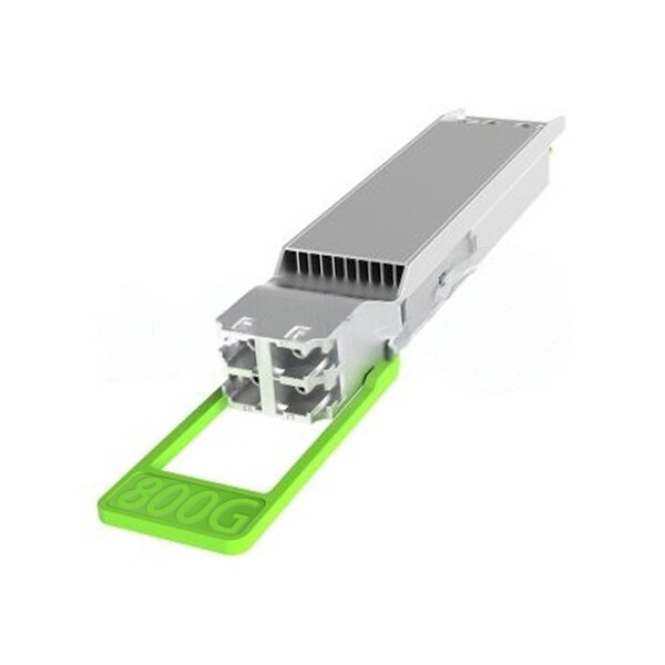
800G and 1.6T Optics
In the 21st century, information technology has developed greatly, and the Internet, big data, and artificial intelligence have greatly enriched people’s communication and life. Today I would like to discuss the transition from 400 Gb Optics to 800 Gb and 1.6 Tb optics in the upcoming years. These transitions are primarily motivated by the changes in service I/O speeds emerging from switch silicon.
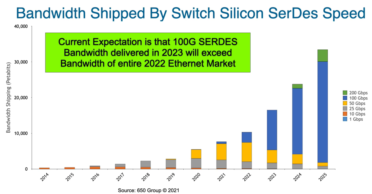
Presently, a significant portion of switch silicon operates at either 25 Gb NRZ or 50 Gb PAM4, utilizing four electrical lanes, which are depicted in gray and yellow on this chart. Commencing from next year, denoted in blue, 100 Gb service will begin shipping and is anticipated to see a substantial increase in volume in 2023.
In fact, projections indicate that the total bandwidth shipped in 100 Gb lanes in 2023 will surpass the entire bandwidth of all shipments in 2022. Looking further ahead to 2024 and 2025, as shown in the graph, the green portion represents the expected early shipments of 200 Gb service I/O.
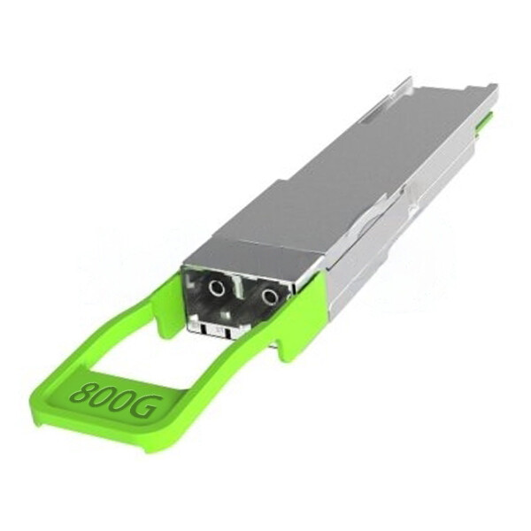
The 100 Gb service speed directly drives 800 Gb optics in the Ethernet optical formats. It’s important to note that the initial emphasis here is on dual 400 Gb and Octo 100 Gb breakout applications. Additionally, there is an Ethernet specification that was completed by the Ethernet Technology Alliance in April of 2020, which will be integrated into switch silicon beginning in 2023. Interestingly, this might be the first instance where 800 Gb optics are readily available in significant production volume before Gb Ethernet becomes available in the market.
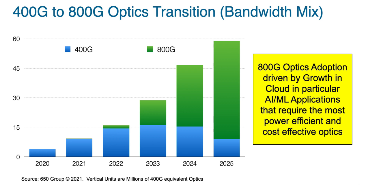
This slide provides a perspective on the expected transition from 100 Gb to Ethernet optics in terms of bandwidth. As you can see, 400 Gb, shown in blue, is still growing steadily for the next two years and is expected to peak in 2023, coinciding with the introduction of 800 Gb optics, depicted in green. It is anticipated that Ethernet optics will become the predominant choice starting in 2024. The predictability of this transition is primarily driven by lower cost, reduced power consumption, and higher density, which are all crucial considerations for both system vendors and customers in the marketplace.
Here is a list of anticipated Ethernet optical modules available in 2023:
- The 800G-ZR module, currently in the design phase, is expected to provide a reach of 100 km or more with 16-QAM modulation.
- The 10km version, known as 800G-LR module, is another option.
- The 800G-FR4and 800G-DR4 module, utilizing 200G-PAM4 for Optical Lambda.
- The 800G-FR8/LR8 module, which is a single fiber with eight channels of 100G
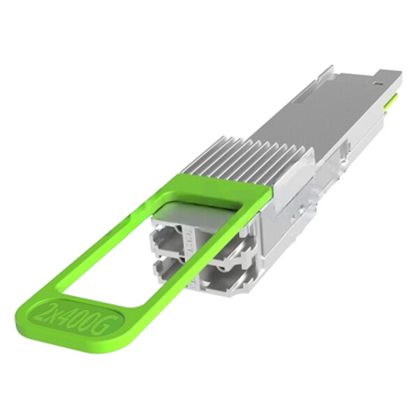
- The Dual FR4 and Dual LR4module for 800G Ethernet and Breakout 2x 400G FR4 Links.
- The 800G-DR8 module with 100G PAM4 and 8-way Single-mode Parallel Technology
- The 800G-SR8 modules can be used in 800G Ethernet, data center links, for 800G-800G interconnections.
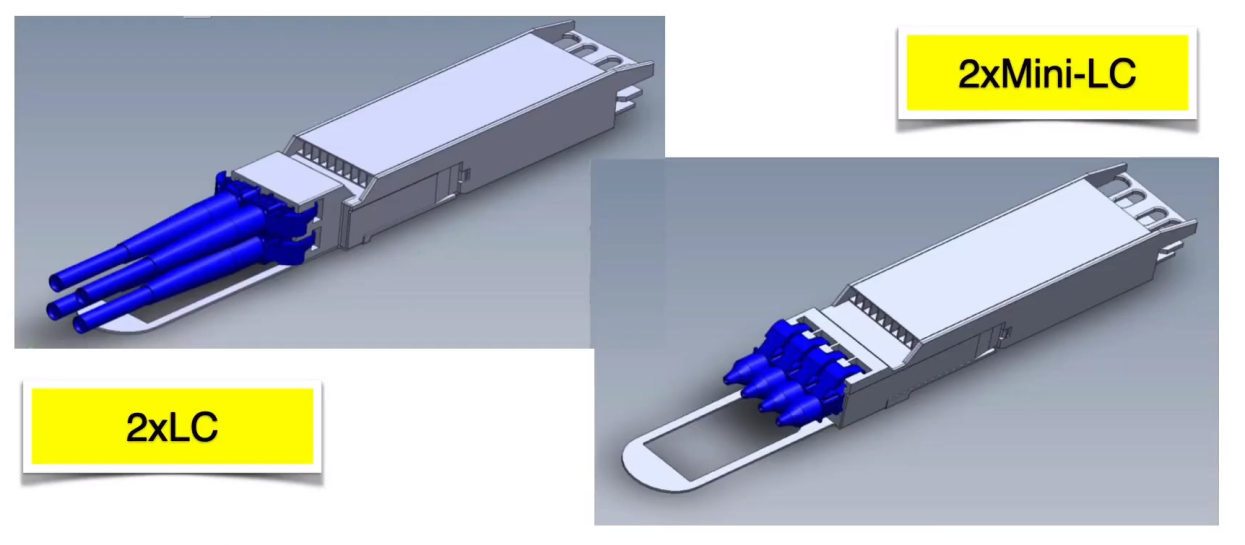
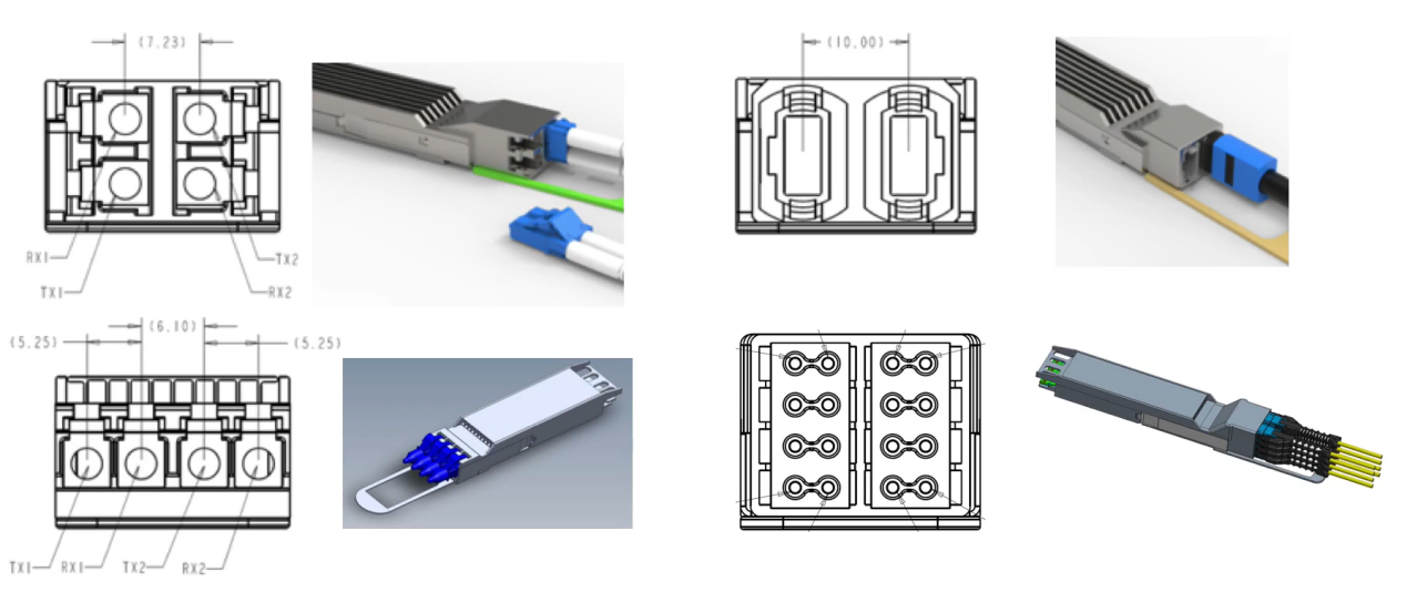
All these optics are expected to hit the market in 2023, with some already in the lab today. Breakout applications are anticipated to be the primary use for these Ethernet modules initially. This aligns with the industry’s need for larger rate on their switch chips, as well as improved compatibility and flexibility. Therefore, it is essential for the optical modules to support standard industry connectors that cater to these breakout applications, including Dual LC, Dual Mini LC, Dual MPO, and Octal breakout into eight SN/MDC connectors.
The image shows an OSFP module with both Dual LC and Dual Mini LC connectors. Several vendors are already working on modules with breakout capabilities, and they should be available in the market by the end of this year.
200G Lambda Optics
Now, moving on to 200G Lambda Optics, there is a growing interest in increasing the speed per Lambda. This advancement promises significant reductions in power consumption, possibly up to 20-30%, and cost savings. Moreover, it is an excellent choice for future Trinity electrical lanes, expected to appear on 102.4T Switch Silicon.
To put the potential cost reduction into perspective, comparing an Ethernet rate module in the lab today with the next-generation 1.6Tb 8x200G Lambda module, which utilizes 800Gb 8x100G Lambda, reveals that they share the same component count. This includes the same number of lasers, modulators, private terminations, connectors, and more. Essentially, the bill of materials supports a significant cost reduction per bit between the 100-Gig generation and the 200-Gig generation.
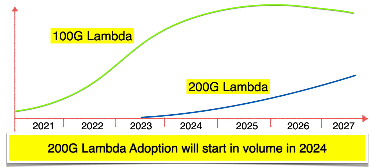
Status of 200G Lambda Optics is currently in early development stages. While technical feasibility has been demonstrated, a complete 200G Lambda specification is still lacking. This specification would include the forward error correction and precise optical specifications for these links, enabling the industry to manufacture and deliver these components.
The adoption of these modules is anticipated to start in late 2023, gather momentum in 2024, and achieve higher volumes in 2025 and beyond. It’s likely that 100G Lambda optics will remain prevalent, possibly through 2025-2026 and beyond.
1.6T Pluggable Optics Modules
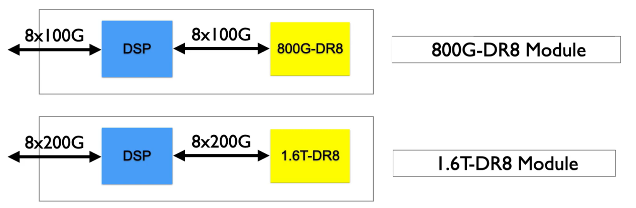
Let me now turn to the 1.6T Pluggable Optics Modules, which involves using 8-channel modules and running them at 8x100G electrical lanes, particularly suitable for OSFP. After research and experimentation, it was found that this approach is not only feasible but can be achieved with minor adjustments in mechanical dimensions, while maintaining full backward compatibility with existing Ethernet OSFP.
It is important to note that these 200G Lambda optics are inherently linked to 200G service switch silicon, expected to be in production by 2025. In contrast, 200G Lambda optics are available much earlier, potentially as early as the second half of 2023. There is considerable interest in bringing 200G Lambda optics to the market as soon as possible, given their potential for cost and power savings.
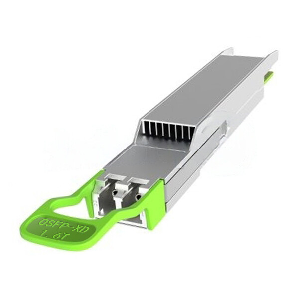
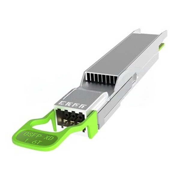
To facilitate this within the context of a low-cost module, the OCFP XD has been recently introduced. This module, denoted as “extra dense” features 16 Gig lanes, effectively adding a second row of connector pins to double the link count. This innovation enables the delivery of a 1.6-terabyte module in conjunction with 51.2T switch silicon in 2023. Remarkably, the density remains the same on the front panel and module side.
As a result, the 51.2T density can fit into a 1U line card or 1U fixed chassis, provided the power requirements align. This approach envisions that a 1.2.4T density with 200G Lambda and 200G electrical interface could also fit into the one uniform connector in the future. This module offers 16 electrical lanes of 100Gb and can be scaled to 1.6 Tb with 200Gb service, with a power specification reaching up to 33W, necessary to support coherent applications.
What’s particularly important is that the footprint of the connector cage for the OCFP-XD matches that of a stacked Ethernet OSFP or SFP, allowing system vendors to design a single motherboard that can be configured with either a stacked Ethernet osfp or SFP connector or with the 1.6-terabyte OCFP-XD. This innovation is expected to expedite adoption significantly.
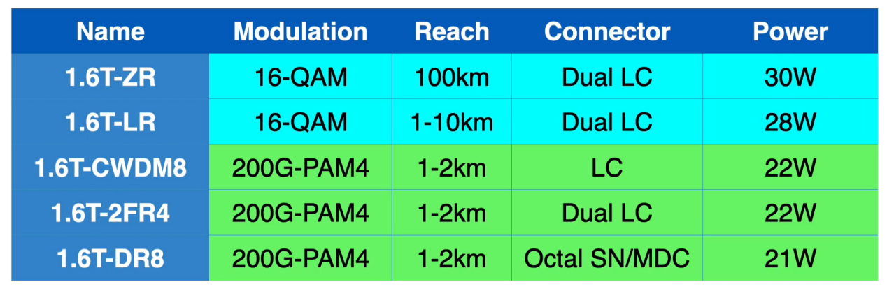
The anticipated modules in the 1.6Tb form factor include 1.6-ZR modules, the LR version with extended reach, CWDM8, which encompasses eight channels of 200G PAM4 over duplex fiber, Dual FR4 will feature dual LCs, and the 1.6T-DR8 an octal SN/MDC connector. Some interest has also been expressed in developing 16-channel in 100G Lambda interfaces.
The OCFP XD offers several advantages, including being the densest pluggable optic solution on the market today. It effectively matches the density of future switch silicon on a 1U front panel basis and supports a wide range of optics technologies, from H100G to 200G Lambda and coherent. Additionally, it retains all the benefits of pluggable optic modules in terms of configurability, serviceability, and technological flexibility.
Reducing Power/Bit
Now, let’s discuss power and how it can be reduced in optics. The Cloud Bandwidth is growing rapidly, estimated to increase by 50-60% per year. Simultaneously, power reductions in optical and network switching are occurring at a rate of 25-30% per year. However, the overall power consumption of the network is still increasing due to the larger growth in bandwidth compared to the reduction in power.
To address this issue, leveraging the most advanced process technology is the most predictable way to achieve power reduction. Expected power reductions from 7 nms to 5 nms to 3 nms are quite significant, nearly a factor of two over two generations. This reduction applies to both the switch chip and the DSP and optics. The power reduction spans the 25.6 switch, 51.2T switch, and the future 1.2.4T switch, with the total system power, including the switch chip, fan power, and optics, decreasing by almost a factor of two over these two generations.
Focusing on optics, the original 400G DR4, which lacked integrated TIA and drivers, had relatively high power consumption per bit. The Ethernet DR4 rate, benefiting from more advanced process technology for DSP and integrated drivers, promises a significant power reduction. When looking at the 1.6Tb generation, expected to employ 3 nm technology, further power reduction is anticipated.
While the power per bit is declining, the power per module is increasing because of the shift from 400G to 800G to 1.6T. As a result, current estimates for 1.6-terabyte data center modules range between 20W and 25W, while coherent DCO modules can go up to 30W per module.
Achieving further power reduction necessitates using 3 nm and beyond, 2 nm DSPs, which provide significant power reduction, particularly on the digital side, including coherent DSPs. It is also essential to design lower-power services, and one should not underestimate the ability of engineers to drive power reduction. Various optics technologies, including lower-power modulation technologies, can help reduce the laser power requirement.
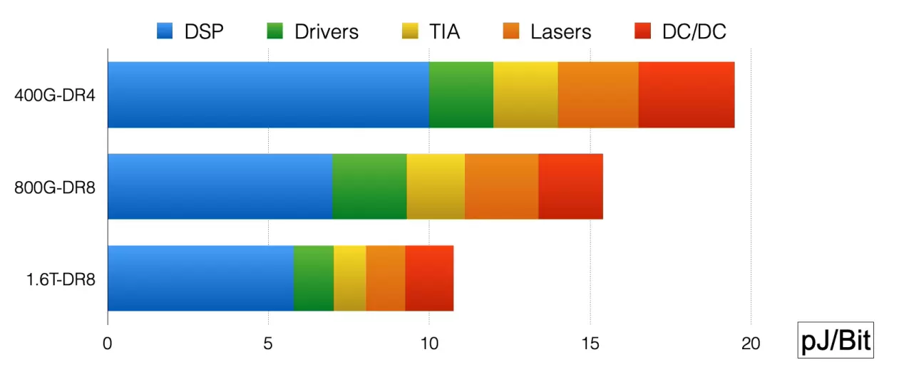
In summary, the industry is actively working on innovations to reduce power consumption in optics. Many advancements have been made, particularly in reducing power per bit, and more are expected in the future, with the potential to achieve 5-6 pJ/Bit by 2026. The ongoing power reduction efforts are independent of the form factor, meaning it applies to both pluggable and co-packaged optics.
Nevertheless, pluggable optics modules allow for more immediate delivery of new components into the install base, which is advantageous in enabling innovation on the optics design side and facilitating the delivery of these innovations to the market.
What about CPO(Co-Packaged Optics)?
Now, let’s delve into the world of co-packaged optics. Describing the current state of co-packaged optics can best be characterized as a work in progress. Considerable headway has been made, thanks to numerous contributions from industry players, including Facebook and Microsoft to the OIF (Optical Internetworking Forum), prototype development, and prototype demonstrations. Challenges, too, are well understood, encompassing laser power, optical losses, connector issues, manufacturability, repairability, and serviceability, among others.
The initial impetus for co-packaged optics was the potential to reduce power consumption on a switch chip and system level by up to 20%, primarily by diminishing electrical lane power—shifting from a high-power LR service to a lower-power XSR service for short-reach connectivity between the silicon chip and the modulator. Regrettably, XSR technology has yet to see practical implementation, making those power savings elusive.
Instead, silicon vendors have developed Very Short Reach (VSR) modes, which, while not as low-power as XSR, have delivered substantial power reductions of up to 180 Watts at the wall-plug level for 51.2T switches, surpassing LR SERDES.
This illustration displays the power levels: traditional LR Serdes in blue, VSR in green, and the targeted XSR in yellow. Though XSR remains a lower-power option, VSR has bridged the gap, and the same interface can be used for both CPU and pluggable optics modules, thanks to fly-over cables.
However, co-packaged solutions using External Light Sources (ELS) to make the laser module replaceable introduce additional optical coupling losses, leading to higher laser power requirements compared to conventional pluggable optical modules. This results from multiple connectors within the co-packaged solution compared to the single connector in a CPU solution with ELS.
Expanded beam connectors are likely needed to prevent dust contamination, and additional splitter and polarization losses contribute to a total additional loss of approximately 1.8 to 3 dB. Consequently, the laser power must increase by 50% to 100%, thereby significantly increasing power consumption. Additional efforts for power reduction are imperative.
Potential solutions include direct drive, which eliminates the need for DSP and utilizes the switch chip’s service to drive the optics directly, delivering notable power savings. On the ELS side, mitigating coupling losses by moving the laser closer to the modulators or exploring different modulation technologies for silicon photonics can contribute to power reduction.
In addition to power considerations, co-packaged optics present challenges related to CPU, such as reliability, serviceability, manufacturability, and testability, as well as business model complexities. It’s worth noting that neither 51.2T nor 102.4T switches require co-packaged optics, as pluggable updates have successfully addressed these demands without risks or design, serviceability, and manufacturing issues. Moreover, current CPO solutions do not yield power savings compared to pluggable optics.
In conclusion, the 800G optics modules are currently under development and target dual 400G and octal 100G breakout applications. The 1.6T optics modules, based on the 16x 100G electrical interface, are next in line, with production possibly commencing in 2023, aiming for the 51.2T switch generation. Subsequently, the 1.6T optics modules using the 8X 200G electrical interface will follow, targeting the 102.4T switch with 200G Serdes, with an estimated production timeline of 2025.
The industry as a whole must maintain its focus on technologies that drive further power reductions, encompassing the most aggressive DSP processes, 200G Lambda, and lower power modulators. While power/bit is decreasing, the power of modules is increasing due to the transition from 400G to 800G and 1.6T.
Thus, the development of a robust thermal solution for 20 to 30-watt optics is essential. In conclusion, decoupling optics transitions from switch silicon provides a significant advantage, allowing for innovation in optics design and rapid integration into existing installations.
Post Views: 23,998