Silicon photonics is a new-generation technology that develops and integrates optical devices using silicon and silicon-based substrates through existing CMOS processes. It is an ideal platform for integrating photonics and microelectronics. As a platform technology, silicon photonics is gaining attention for its high speed, high integration, low cost, low power consumption, and compact size. It is now widely used in optical communication, optical sensing, optical computing, autonomous driving, and consumer electronics.
The development of artificial intelligence (AI), from early decision-making intelligence to today’s generative intelligence and future agent-based intelligence, all relies on “training” computing systems to give them intelligent capabilities.
So-called “10,000-card clusters” or “100,000-card clusters” refer to computing networks made up of tens of thousands of AI chips used for training tasks. This is similar to how the human brain gains knowledge by reading many books.
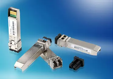
In this process, optical modules handle data transmission, while optical fibers serve as the transmission channels. Besides silicon photonics, other optical interconnect solutions include cable modules, VCSEL-based multimode modules, and EML-based single-mode modules.
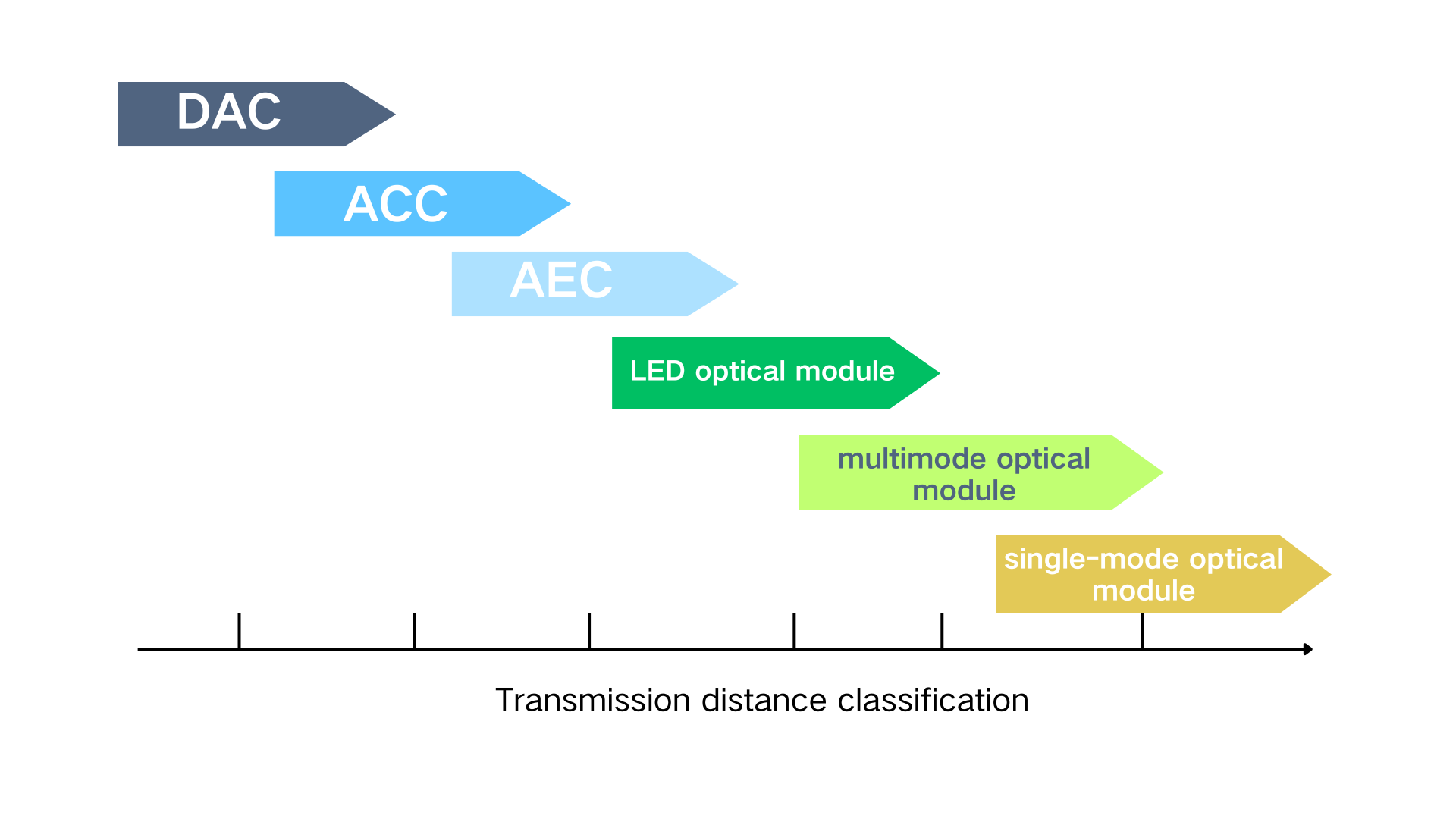
Optical module classification by transmission distance
Overview of Silicon Photonics Technology
Silicon photonics uses silicon and silicon-based substrate materials (such as SiGe/Si and SOI) as optical media. It relies on CMOS-compatible integrated circuit processes to manufacture photonic and optoelectronic devices, including silicon-based light sources, modulators, detectors, and waveguide components. These devices are used to emit, transmit, detect, and process light signals, enabling practical applications in fields such as optical communication, optical sensing, and optical computing.
Silicon photonics is increasingly integrated and applied across more fields. It uses silicon and silicon-based substrates as optical media and employs CMOS integrated circuit processes to manufacture photonic and optoelectronic devices. These enable practical applications in areas such as optical communication, sensing, and computing. As integration density rises, the number of integrated components grows, and application scenarios continue to expand.
According to LightCounting, the market share of optical modules based on GaAs and InP is expected to decline, while silicon photonics (SiP) and thin-film lithium niobate (TFLN) PICs are projected to gain ground. The adoption of LPO and CPO will also help boost the market share of SiP and even TFLN devices. LightCounting predicts that sales of silicon photonic chips will grow from $800 million in 2023 to just over $3 billion by 2029.
Silicon photonics can be used in both traditional pluggable optical modules and CPO (co-packaged optics) solutions. At the 800G transmission rate, the adoption of silicon photonics in packaging is expected to increase, while CPO remains more of a technology exploration at this stage. However, starting from 1.6T, traditional pluggable modules may reach their performance limits, and future optical interconnect upgrades may shift toward CPO and coherent solutions.
Advantages of Silicon Photonics
First, it’s important to clarify a common misconception: the core advantage of silicon photonics is not a higher single-channel data rate.
EML (Electro-absorption Modulated Laser) technology dates back to the 1980s and is based on InP materials. The industry has a well-established theoretical and practical foundation for designing EML using InP, and data rates have already reached 448Gbps (PAM4 signal, requiring around 110GHz bandwidth).
In comparison, achieving 200Gbps with silicon photonic modulators (PAM4, needing about 60–70GHz bandwidth) remains technically challenging. Thin-film lithium niobate (TFLN) modulators, on the other hand, can also reach 448Gbps.
In the competition between silicon photonics and EML, the key advantages of silicon photonics lie in the following aspects:
Easier integration
One of silicon photonics’ main strengths is its ease of integration.
EML uses compound semiconductor materials like InP, which require butt-joint epitaxial growth. The internal DFB laser must also meet single-mode requirements. Due to these factors, only a small portion of EML chips on a wafer meet the required standards — they must be “selected” as good chips. While EML integration is technically feasible (for example, Mitsubishi has developed a dual-EML integrated chip), the yield of integrated arrays drops sharply because of the low yield of individual EML chips.
In contrast, silicon is a single-element semiconductor. It doesn’t need epitaxial growth or complex quantum well bonding, making the manufacturing process more straightforward and yielding higher chip quality. Integrating multiple modulators, detectors, WDM components, and even hybrid-integrated lasers is relatively more feasible with silicon photonics.
In a silicon photonic integration system, it’s not just about integrating multiple modulators. It can also include the integration of multiple modulators with multiple detectors, as well as combining these with wavelength division multiplexing (WDM) components. At a more advanced level, it may also involve hybrid integration with lasers—bringing together modulators, detectors, WDM components, and light sources into a higher-dimensional integrated system.
Its larger RF bandwidth for electrical signals
EML chips themselves are not large, but they are packaged one by one with individually coupled optical paths. Each chip requires careful electrical design for data rate, impedance, and termination, which results in a large number of peripheral components. Production and testing must be done individually, making the manufacturing process of optical modules more complex and time-consuming. Although EML chips are physically smaller (less than 1mm in length, width, and height) than silicon photonic chips, their packaging and system integration are more complicated.
Silicon modulators do not offer as wide a bandwidth as EML—for example, current industry implementations can reach around 55GHz, which is suitable for modulating a single-lane 200G PAM4 signal.
However, since silicon is widely used in integrated circuits, it benefits from mature processes in electrical signal handling. Its precise etching capabilities also enable high-speed electrical interconnects (also known as RF signals) with relatively large bandwidth, which supports efficient signal transmission within the silicon photonic system.
EML uses electro-absorption modulators, many of which have achieved bandwidths exceeding 100GHz, according to various manufacturers. In contrast, traditional packaging processes used to connect EML chips typically limit electrical signal bandwidth to around 50–70GHz. This is why EML manufacturers are working to improve packaging bandwidth—for example, by using flip-chip (FC) bonding instead of wire bonding.
In the competition between silicon photonics and EML within AI applications, both technologies serve similar use cases but come with their own strengths and weaknesses. Their relationship is both unified and competitive.
Thin-film lithium niobate (TFLN) offers a promising alternative—it can be integrated and even bonded onto a silicon substrate, leveraging mature silicon IC post-processing techniques. It combines the advantage of wide modulator bandwidth with strong RF signal handling capabilities. However, TFLN manufacturing processes are still less mature compared to those of silicon photonics and InP.
3D packaging of optical and electrical integration
Silicon has a strong foundation in the integrated circuit industry. Although the optical performance of silicon photonic devices—such as modulation efficiency and stability—still has room for improvement, 3D integration of silicon photonic chips with electronic chips is a key strength of the technology.
The main packaging challenges in silicon photonics lie in the optical components, such as the design and stability of optical modulators (e.g., Mach-Zehnder or microring types), and efficient coupling between the silicon photonic chip, optical fibers, and continuous-wave (CW) lasers.
Its potential for low cost and high density in the future.
Silicon wafers are large, commonly 8-inch or 12-inch in diameter (with 12-inch being 300 mm). In contrast, InP chips typically use smaller wafers—2-inch or 3-inch (3-inch equals 75 mm), though there are also efforts toward 6-inch InP wafers. If the silicon photonics industry continues to scale and optical processes mature, mass production could lead to significant cost reductions.
Silicon waveguides are very compact—smaller than InP waveguides and also smaller than those in current thin-film lithium niobate devices. They have tight bending radii, which enables higher component density and miniaturization under the same integration level (such as integrating the same number of modulators).
It’s worth noting that a single EML chip (e.g., a 200G EML with an electro-absorption region of about 80–100 μm) is usually smaller than a silicon photonic modulator (e.g., a 200G silicon MZ modulator with a modulation region of 1–2 mm). However, in terms of overall system integration density, silicon photonics holds a stronger advantage.
Advantages of Silicon Photonic Modules
Silicon photonic modules can overcome the transmission limitations of traditional single-channel optical chips, offering significant advantages for the era of high-speed data transmission. Compared with traditional discrete optical modules, silicon photonic modules also feature lower cost, lower power consumption, CMOS process compatibility, and higher integration.
At present, commercial optical integration technologies mainly fall into two camps: III-V and silicon (Si). Lasers such as DFB, DML, and EML belong to the InP-based III-V camp. Although this technology is relatively mature, it comes with high costs and is not compatible with CMOS (integrated circuit) processes. InP substrate production also doubles only every 2.6 years.
In contrast, silicon photonic devices use CMOS processes to monolithically integrate passive optoelectronic components and integrated circuits. This allows for large-scale, high-density integration. The production capacity of silicon substrates can double every year, offering a faster scaling advantage.
Traditional optical modules
Silicon photonic modules
Advantages
1. High coupling efficiency
2. Cost advantage in low-speed transmission;
3. Easy to integrate with other optical transmission systems.
1. High integration: Based on CMOS processes, with tight integration of modulators and passive optical paths;
2. Breaks through the speed limits of single-channel optical chips, offering performance advantages for high-speed transmission;
3. Silicon-based substrates offer significant potential for cost reduction.
Disadvantages
1. III-V optical chips are expensive;
2. They use a discrete structure, leading to high packaging costs and low integration density.
1. Silicon waveguides have low coupling efficiency with optical fibers and higher loss, making them more suitable for short- to medium-distance transmission;
2. Integrating III-V compound materials on silicon poses compatibility challenges, resulting in lower silicon wafer yields;
3. There is no cost advantage before 400G.
Future Outlook
With the rapid advancement of AI, optical communication networks are continuously evolving toward higher speeds such as 1.6T and 3.2T, creating growth opportunities for the silicon photonics industry. In the data center market, high-speed optical modules are upgrading rapidly, and silicon photonics adoption is expected to increase. In the telecom market, as coherent optical modules continue to evolve, the demand for silicon photonic modules may also grow.
In the field of CPO, silicon photonics—one of its core technologies—is expected to benefit significantly from growing CPO demand and become a strategic focus for major players. In the OIO (optical I/O) space, as AI continues to drive computing power requirements, the volume of data exchanged between chips is increasing. OIO’s technical advantages are becoming more prominent, and silicon photonics, as an ideal platform for OIO, is also expected to see further development.
(2) Silicon Photonics CW Light Source Providers:
The integration of light sources remains one of the major technical challenges in silicon photonics. Currently, external CW (continuous-wave) lasers are the mainstream solution for silicon photonic modules and are also applicable in CPO and other scenarios. As demand for higher optical transmission rates increases, the number of channels in silicon photonic modules continues to rise, driving further growth in CW light source demand.
(3) Silicon Photonics Process Equipment Suppliers:
Silicon photonics manufacturing processes are increasingly converging with microelectronics. As silicon photonics becomes more widely adopted, supporting investments in process equipment and software vendors will become increasingly important for the ecosystem.
Conclusion
Silicon photonic integration is a key enabling technology to overcome the core bottlenecks of data transmission bandwidth and energy efficiency in current and future AI computing systems. By offering ultra-high bandwidth and ultra-low power optical interconnects, it significantly enhances the performance and energy efficiency of large-scale AI clusters. At the same time, it provides a hardware foundation for exploring disruptive AI computing paradigms such as optical neural networks.
As the technology continues to mature and costs keep decreasing, silicon photonic integration is expected to play an increasingly vital role in AI accelerator cards, data center interconnect networks, and future dedicated optical computing chips—becoming one of the core engines driving the ongoing evolution of AI.