Optimized Design of 400G Optical Transceiver Module
June 17, 2025
With the widespread application of cloud computing and big data, large-scale data centers have become one of the most critical infrastructures for the future digital industry, and their number is increasing rapidly. The computing power and internal data exchange capacity of data centers are also growing exponentially.
Since optical modules are commonly used for interconnecting servers and switches within data centers, they serve as the core components of optical interconnects, playing a decisive role in the operational quality of the entire communication system. Therefore, designing higher-speed optical module products while ensuring their performance and stability is crucial.
This paper presents an optimized design for the optoelectronic packaging and thermal management structure of the 400G optical transceiver module (hereinafter referred to as the optical module).
Among 400G optical transmission products, optical modules have the highest demand. Each module incorporates 16 transmission channels (8 for transmitting and 8 for receiving), with each channel operating at a data rate of 50 Gb/s using 4-level pulse amplitude modulation (PAM4), collectively enabling bidirectional transmission at 400 Gb/s. The overall block diagram of the optical module is shown in Figure 1.
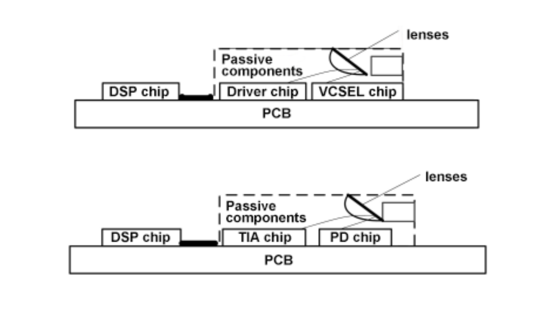
The electrical section primarily consists of a digital signal processing (DSP) chip, transimpedance amplifier (TIA) chips, and laser driver (Driver) chips. The optical section and passive optical components mainly include vertical-cavity surface-emitting laser (VCSEL) chips, photodiode (PD) detector chips, and optical lenses.
At the transmitter (TX) end, electrical signals enter the PAM4 DSP chip from the connector interface for signal conditioning. The processed high-frequency signals are then split into two groups of four channels and fed into the Driver chips. The Driver chips amplify the signals and drive the VCSEL chips to perform electrical-to-optical (E/O) conversion.
At the receiver (RX) end, optical signals enter the PD chips via the MPO-16 optical interface. The PD chips generate corresponding photocurrents, which are then amplified and amplitude-shaped by the TIA chips before entering the DSP chip. Within the DSP chip, the high-frequency signals are reshaped and output, thereby completing the optical-to-electrical (O/E) conversion.
Figure 1 shows the overall optoelectronic layout and structural schematic of the module. During manufacturing, a high-precision chip mounter is used to place the Driver, TIA, VCSEL, and PD chips onto the printed circuit board (PCB). These chips are then interconnected using a high-precision wire bonder to establish electrical signal paths. During bonding, the loop height of the bonding gold wires was minimized, significantly shortening their length and reducing the impact of high-speed signal reflections.
At the TX end, the top surfaces of the Driver and VCSEL chips are positioned on the same plane. Similarly, at the RX end, the top surfaces of the TIA and PD chips are aligned on the same plane. This configuration effectively shortens the bonding wire lengths. Thermal vias directly connect the gold-plated areas under the electrical chips to the backside of the PCB. High thermal conductivity material is filled into the backside openings and contacts the metal housing, creating an efficient thermal dissipation path.
Furthermore, gaps between the circuit chips and the metal housing are filled with high thermal conductivity material to achieve excellent thermal management performance. After integrating the optical and electrical chips, a passive optical component incorporating lenses is used for integrated optical coupling and hermetic sealing of the optical engine at both TX and RX ends. Compared to passive components without lenses, this lens-integrated design improves coupling efficiency by 10% to 15%.
Figure 1 Overall Optoelectronic Layout and Structure of Optical Modules
High-Frequency Electrical and Optical Design of the Optical Module
PCB Design of the Optical Module
The module’s PCB employs a 10-layer stackup, with 4 layers dedicated to high-frequency differential traces and the remaining 6 layers serving as reference and DC power planes. Impedance calculation software (Polar SI9000) and 3D electromagnetic field simulation software (HFSS) were used to calculate the impedance of the high-frequency differential traces and perform simulation tests (Under an outer-layer differential structure, a 100Ω impedance differential pair requires a trace width of 4 mil and spacing of 8 mil).
For the high-frequency differential signal layers, low-dielectric-constant, high-speed specialty laminates (e.g., Rogers or Panasonic M6) must be used. Additionally, to ensure physical symmetry across the stackup and prevent PCB warping due to uneven heating, the laminate stack was designed symmetrically. The reference and DC layers in this module design utilize standard FR4 material.
High-Frequency Circuit Analysis and Optimization
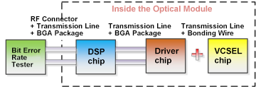
The Input/Output Buffer Information Specification (IBIS) model was employed for simulation and design. In the TX structure of the optical module, a bit error rate tester (BERT) generates 26.5625 GBaud high-speed differential signals. These signals are connected to the module’s test board via a 40 GHz bandwidth cable and a sub-miniature high-frequency connector (2.92 mm connector).
The signals are then transmitted through a Quad Small Form-factor Pluggable – Double Density (QSFP-DD) connector on the test board to the DSP chip inside the optical module. Within the module, the DSP chip recovers and reshapes the high-speed signal data before transmitting it to the Driver chip. The Driver chip amplifies the signals and drives the VCSEL chip to generate optical signals. A block diagram of the TX equivalent circuit structure is shown in Figure 2.
Figure 2 Equivalent Circuit Diagram of Transmitter-Side Packaging
Areas such as the gold fingers and coupling capacitors cannot achieve perfect continuity for high-frequency signals. Therefore, this work focused on optimizing the high-frequency performance of the circuits from the module’s gold fingers to the DSP chip and from the DSP chip to the Driver chip. The gold finger contact points were designed according to the QSFP-DD Multi-Source Agreement (MSA) standard. Gold plating and nickel-palladium-gold (ENEPIG) processes were applied to the gold fingers to enhance wear resistance and conductivity, thereby reducing signal leakage.
Furthermore, the inductance of the circuits was increased by widening the spacing between the multi-layer electrical reference planes surrounding the signal traces and the signal vias, helping to reduce signal reflections. Using a localized trimming method within the simulation software, the 16 pairs of high-frequency lines from the gold fingers to the DSP chip were trimmed and simulated. Impedance calculation software was then used to adjust the trace thickness, width, and spacing for each high-frequency line pair.
For the coupling capacitors, their placement was primarily adjusted based on simulation results. Ground reference vias were placed at the four corners of the entire model to create a return path for interference signals, achieving anti-interference objectives.
High-frequency optimization results showed that all 32 sets of high-speed differential lines (TX and RX combined) meet the requirement of a 3 dB bandwidth greater than 35 GHz (the actual operating bandwidth is less than 20 GHz). The impedance of all high-frequency lines is controlled at 100 Ω (with an error tolerance of ±1 Ω), and the return loss values are all less than -15 dB.
Additionally, the VCSEL chips are connected to the Driver chips via differential bonding wires using standard 25 μm diameter gold wire. The length of the longest bonding wire was reduced from 500 μm to 280 μm, decreasing the insertion loss by 0.3 dB.
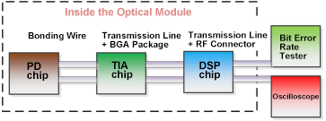
Figure 3 shows the structural schematic of the receiver (RX) end. The optimization process for the high-frequency differential lines on the RX end was similar to that on the TX end. The trimming method was applied: each differential pair was trimmed, modified, simulated, optimized, and then modified again until it met the specifications. After optimization, the impedance of all differential lines is precisely controlled at 100 Ω (±1 Ω tolerance), the 3 dB bandwidth meets the 35 GHz requirement, and the return loss is less than -8 dB.
Figure 3 Structural Block Diagram of Receiver-Side Packaging
Optical Design
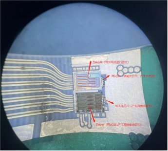
Figure 4 shows the finished photo of the module after die attach and wire bonding. A chip mounter was used to place the Driver and TIA chips onto the PCB according to pre-defined placement markers, ensuring a placement accuracy error of less than 3 μm. This precision is crucial for product accuracy and optical coupling stability. After placing the Driver and TIA chips, the VCSEL and PD chips were placed, aligning them precisely with the corresponding working areas of their respective Driver and TIA chips. Alignment followed the Ground-Signal-Ground (GSG) pad positions, also with a placement error of less than 3 μm. After die attachment, bonding parameters (wire length and angle) derived from simulations were set, and all pads were wire bonded, completing the electrical connection between the chips and the PCB.
Figure 4 Finished Image of Optical Module Surface-Mount Bonding
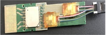
Following wire bonding, high-precision active alignment coupling was performed using a coupling machine. The coupling process was conducted in two stages: First, one set of Driver and TIA chips was coupled (using an optical power meter to detect the output power of 4 TX channels and software to detect the responsivity of 4 RX channels).
Once the detection metrics for both TX and RX simultaneously reached their maximum values, the lens was fixed in place using adhesive. The second set of chips was then coupled and fixed using the same procedure. A photograph of the fabricated 400G optical transceiver module is shown in Figure 5.
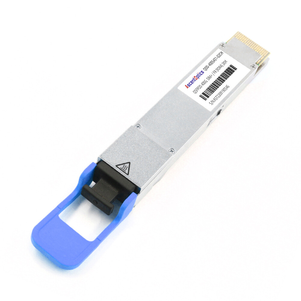
Figure 5 Physical Diagram of 400G Optical Transceiver Module Structure
Optical Module Simulation and Testing
Optical Module Link Simulation Structure
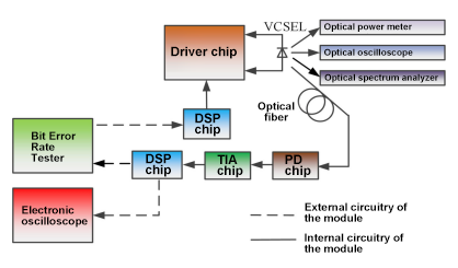
Figure 6 illustrates the schematic of the optical module link simulation structure. At the transmitter (TX) end, the VCSEL emits light driven by the Driver chip. The high-speed RF signal output from the Driver chip modulates this light. Instruments such as an optical power meter, optical oscilloscope (sampling oscilloscope), and optical spectrum analyzer (OSA) are used to measure key parameters of the optical signal, including average optical power (P<sub>avg</sub>), extinction ratio (ER), and wavelength.
For module loopback or cross-testing, the received optical signal at the RX end undergoes processing through the PD, TIA, and DSP chips. The resulting electrical signal is then sent to an electrical oscilloscope to observe the converted signal eye diagram and analyze signal quality. Feeding this signal into the RX port of a bit error rate tester (BERT) allows the real-time bit error rate (BER) to be read, determining if the module’s transmission quality meets international standards.
Figure 6 Schematic Diagram of Optical Module Simulation Link Structure
Module Testing
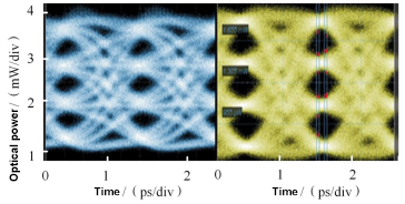
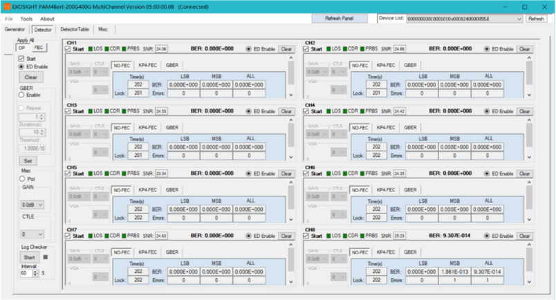
The 400G optical transceiver module underwent eye diagram testing and bit error rate measurement. The eye diagram and BER plot are shown in Figure 7 and Figure 8, respectively. Test results indicated that the module exhibits a clear eye diagram with a jitter of approximately 2.3 ps. Good consistency was observed across all channels, with zero errors recorded over a 202-second period.
Figure 7 Eye Diagram from Optical Module Testing
Figure 8 Bit Error Rate (BER) Diagram from Optical Module Testing
Additionally, the system transmission performance of the 400G optical transceiver module was tested over a 100-m distance. The eye diagrams for each channel showed minimal difference compared to direct connection (0m) test results.
Although the average jitter increased slightly, channel-to-channel eye diagram consistency remained good. At a transmission rate of 50 Gb/s per channel, no packet loss occurred, indicating stable system performance. The total power consumption of the entire optical module was measured at 9.8 W, demonstrating relatively low power consumption.
Conclusion
This paper presented a systematic design of the structure and high-frequency circuits for a 400G optical module, optimized using specialized software. Test results confirmed that compared to using passive components without lenses, the lens-integrated passive components improve coupling efficiency by 10% to 15%. After high-frequency circuit optimization, the return loss values are all less than -15 dB, and insertion loss was reduced by 0.3 dB.
The optical transceiver module exhibits a clear eye diagram with a jitter of about 2.3 ps and demonstrates good channel-to-channel consistency, achieving zero errors over 202 seconds. After 100 m signal transmission, the bit error rate remains below 1E-12. With a total power consumption of 9.8 W, the module meets international standard requirements.
Reference Sources
Optimized Design of 400G Optical Transceiver Module
Authors: NIE Song, JIA Jiangang, LIU Chao
Published: 2023
Journal: Optical Communication Technology
Abstract: In order to further improve the optical coupling efficiency and output power of the optical module, a 400G optical transceiver module is designed and optimized. A passive device with a lens is used as an important part of the optical coupling to improve the coupling efficiency. The input/output buffer information specification (IBIS) model is used to analyze and optimize the high frequency circuit of optical module. Finally, the optical design, link simulation and test of the optical module are carried out. The test results show that the designed optical transceiver module eye image is clear, the optical eye image jitter is about 2.3 ps, each channel has a good consistency, no error code within 202 s. After the signal is transmitted for 100 m, no packet loss occurs, and the system performance is stable.