With the rise of new technologies such as 4K virtual reality (VR), Internet of Things (IoT), and cloud computing, the demand for network bandwidth, concurrency capabilities, and real-time performance is becoming increasingly urgent. According to Omdia’s predictions, bandwidth demand will continue to rise in the coming years. Although 100, 200, and 400G optical modules will still dominate the market, 800G optical modules will achieve commercialization by 2023, and are expected to achieve large-scale deployment by 2025.
In the 800GE network architecture shown in Figure 1, the connection distance between the top-of-rack switch (TOR) and the Leaf switch ranges from tens of meters to hundreds of meters. Currently, large internet companies generally adopt 100Gbit/s connection technology, and have been gradually upgrading to 200Gbit/s or 400Gbit/s since 2021. Some leading companies are expected to try 800Gbit/s technology in 2023.
The connections between Leaf switches and Spine switches, or between Spine switches and core routers, address the interconnectivity challenges within or between adjacent campus areas. The distances for these connections can extend up to 2km, or even 10km. Interface speeds are also set to gradually upgrade to 200Gbit/s or 400Gbit/s starting from 2021. Certain companies are planning to commence trials of 800Gbit/s technology in 2023.
Data Center Interconnect (DCI) typically refers to load balancing or disaster recovery backup connections between adjacent data centers, with connection distances that can span several tens of kilometers. Given the valuable nature of optical fiber resources, people commonly employ techniques like DWDM and coherent communication to maximize the reuse of optical fiber resources. The application scenarios for 800G optical modules include SR (100m scenario), DR/FR/LR (500m/2km/10km scenarios), as well as ER/ZR (40km/80km scenarios).
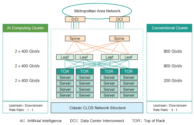
Figure 1 800GE Networking Structure
The evolution of the 800Gbit/s technology solution includes three generations.
Generation 1: 8 Optical 8 Electrical- Optical interface 8x100Gbit/s, Electrical interface 8x100Gbit/s, commercially available since 2021.
Generation 2: 4 Optical 8 Electrical – Optical interface 4x200Gbit/s, Electrical interface 8x100Gbit/s, expected to be commercially available in 2024.
Generation 3: 4 Optical 4 Electrical – Optical interface 4x200Gbit/s, Electrical interface 8x100Gbit/s, expected to be commercially available in 2026.
In the long term (within the next 5 years), single-channel 200Gbit/s optical/electrical technology is expected to become widely adopted. However, in the short term (within the next 3 years), due to the immaturity of optical-electrical chip components and equalization techniques for single-channel 200Gbit/s, the industry will require some time to overcome the related technical challenges.
Looking at the development of 100Gbit/s direct detection optical modules, when the electrical interface single-channel rate matches the optical interface single-channel rate, the architecture of the optical module will achieve optimal performance. This will result in advantages such as low power consumption and low cost.
Following this trend, a single-channel 100Gbit/s electrical interface is poised to become the ideal choice for 8x100G optical modules, while a single-channel 200Gbit/s electrical interface holds potential to be the ideal option for 4x200G optical modules.
In terms of form factor, 800G optical modules might adopt various forms such as Dual Density Quad Small Form Factor Pluggable (QSFP-DD800) and Octal Small Form Factor Pluggable (OSFP). However, due to factors like internal module wiring and connector losses, pluggable optical modules based on 200Gbit/s electrical interfaces still face some challenges.
The optical interface architecture of 800G optical modules primarily consists of three types, as depicted in Figure 2.
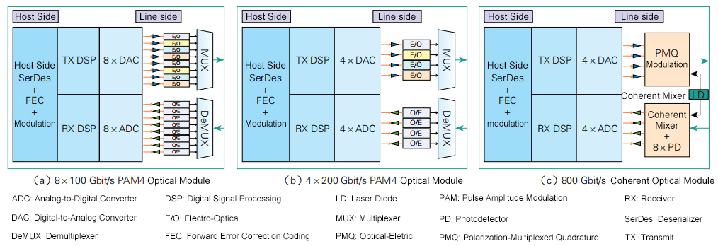
Figure 2 Three types optical interface architecture of 800G optical modules
(a) The optical module solution utilizing 8x100Gbit/s 4-level Pulse Amplitude Modulation (PAM4) technology is as follows: In this scheme, PAM4 transceivers operate at a rate of 53Gbd. It consists of 8 pairs of digital-to-analog converters (DAC) and analog-to-digital converters(ADC), 8 lasers, and 8 pairs of optical transceivers.
Additionally, the scheme also includes 1×8 channel Coarse Wavelength Division Multiplexing (CWDM) or LAN-WDM (based on Ethernet channels) devices, depending on the optical fiber’s dispersion loss characteristics. These devices facilitate multiplexing and demultiplexing functions (typically not required in SR/DR application scenarios).
(b) The scheme for the 4x200Gbit/s PAM4 optical module is as follows: In this scheme, PAM4 transceivers operate at a rate of 106Gbd. utilizing 4 sets of Digital-to-Analog Converters (DACs) and Analog-to-Digital Converters (ADCs), as well as 4 pairs of optical transceivers (including 4 lasers). Additionally, the scheme also includes 1×4 channel Coarse Wavelength Division Multiplexing (CWDM) or LAN-WDM (based on Ethernet channels) devices, depending on the optical fiber’s dispersion loss characteristics. These devices facilitate multiplexing and demultiplexing functions (typically not required in SR/DR application scenarios).
(c) The scheme for the 800G coherent optical nodule is as follows: Operating at a rate of 128 Gbd in Dual Polarization Sixteen-Quadrature Amplitude Modulation (16QAM) mode, this optical module employs 4 sets of Digital-to-Analog Converters (DACs) and Analog-to-Digital Converters (ADCs), as well as 1 laser and 1 pair of optical transceivers. It’s worth nothing that this module can utilize fixed-wavelength lasers in coherent optical communication within data centers, aiming to reduce costs and power consumption.
In the context of long distances, the development of 800G coherent optical modules encompasses multiple aspects:
(1) Challenges and Developments in Multi-mode Solutions:
In short-distance (SR) scenarios, the 100Gbit/s technology employing Vertical Cavity Surface Emitting Lasers (VCSELs) faces challenges. Enhancing the performance of multi-mode solutions while reducing the cost on multi-mode fiber will be crucial for technological advancement. Simultaneously, single-mode technologies based on Silicon Photonics (SiPh) and Direct Modulation Lasers (DML) are rapidly evolving in DR/FR scenarios. SiPh technology is progressing rapidly and may compete with multi-mode solutions, especially in applications with transmission distances of 100m and below.
(2) Competition In Single-Mode Solutions:
In DR/FR scenarios, three solutions are competing: Electro-Absorption Modulated Lasers (EML), Direct Modulation Lasers (DML), and Silicon Photonics (SiPh). In LR scenarios, the 800Gbit/s LR8 solution based on Coarse Wavelength Division Multiplexing (CWDM), Long Wavelength Division Multiplexing (LWDM), and narrowband Long Wavelength Division Multiplexing (LWDM) is still in the research phase. Regarding wavelength selection, LWDM8 offers dispersion advantages over CWDM8, but currently faces challenges in dispersion and dispersion tolerance matching.
(3)Dispersion Challenges and Solutions:
For the direct detection schemes over long distances (10km and above), one of the main challenges is the matching of “worst-case”dispersion and narrow dispersion tolerance. Building new wavelength schemes and compressing the wavelength range for multiple channels can reduce the dispersion range, simplify Digital Signal Processing (DSP) design, and lower power consumption. For instance, employing wavelength division multiplexing schemes with different spacing can achieve various dispersion-limited distances.
(4)Bandwidth Demand Increase and Technological Challenges:
The bandwidth requirements for 800G coherent optical modules need to be enhanced, but achieving a doubling of bandwidth in device design is not feasible in a single step. Device designs based on higher bit rates enable higher-order modulation formats, but they might encounter limitations in terms of signal-to-noise ratio and transmission distance. In this regard, coherent optical modules based on 128GBd dual-polarization (DP) 16QAm modulation hold promise as the primary implementation solution for 800G coherent communication due to their superior optical signal-to-noise ratio and transmission capabilities.
In general, the development of 800G coherent optical modules involves multiple technological directions, encompassing both multi-mode and single-mode approaches. These approaches face challenges across various transmission distances and application scenarios. To achieve higher performance and efficiency, continuous research and innovation are essential.
Forward Error Correction (FEC) technology can be broadly categorized into three types: end-to-end FEC, concatenated FEC, and segmented FEC. For optical communication solutions, selecting the appropriate FEC scheme is crucial based on the varying transmission distances and requirements.
In specific implementations, for the 8x100Gbit/s direct detection scheme within a 40km transmission distance, an end-to-end KP4 FEC scheme can be employed. However, for longer transmission distances, a stronger FEC encoding scheme might be necessary. For the 4x200Gbit/s direct detection scheme, due to its higher data rate, it requires the introduction of new BER standards, FEC coding methods, and more complex equalization techniques.
The IEEE 802.3 B400G SG and 800G Pluggable MSA working groups have initiated discussions on these relevant issues, and the concatenated approach could potentially become a new path for the 4x200Gbit/s direct detection scheme.
This concatenated approach not only retains the benefits of KP4 FEC, avoiding the additional costs associated with integrating new FEC into the main chip, but also provides additional protection to the optical link through the lightweight and easily implementable FEC within the optical module. This approach helps reduce the power consumption and latency introduced by decoding.
In terms of error correction performance, employing various concatenated inner codes such as KP4+BCH (144,136) can narrow the post-correction range to less than 1E-13 within a range of pre-correction bit error rate of 1 to 2E-3.
Currently, the most demanding requirements for 800Gbit/s stem from applications such as OTT (Over-The-Top) data centers and high-performance computing, which are particularly sensitive to latency. Consequently, low-latency FEC algorithms have become one of the core requirements for 800Gbit/s optical communications.
The 800G coherent optical communication solutions encompass two scenarios: 800Gbit/s LR and 800Gbit/s ZR. Consequently, tailored FEC algorithms are necessary for different application scenarios. In the 800LR scenario, a 10km campus network is required, placing high demands on latency and power consumption.
Current solutions include concatenated schemes like KP4+eHamming/eBCH, spatially coupled FEC (XR-FEC), cluster FEC (CFEC), Zipper, and lightweight open FEC (OFEC), among others. Among these, the concatenated approach shares similarities with the concatenated scheme for 4x200Gbit/s direct detection, allowing for reduced complexity of the main chip.
In the 800ZR scenario, mainly applied to Data Center Interconnect (DCI), the continuation of the Optical Internetworking Forum’s (OIF) 400ZR standard is observed. 800ZR employs DP-16QAM modulation format, which could pose challenges to the error correction capabilities of CFEC. This might necessitate the adoption of stronger FEC schemes such as multi-level coding (MLC) or OFEC, which offer enhanced error correction capabilities.
To achieve a data transmission rate of 200Gbit/s per single channel, performance upgrades are required for optoelectronic chips. These upgrades include the necessity for a 200Gbit/s SerDes, optoelectronic chips, and devices with bandwidth exceeding 50 GHz. Current technology research reports indicate that achieving optoelectronic chips with bandwidth exceeding 50 GHz is relatively feasible.
However, while increasing bandwidth, ensuring optimal performance across other metrics becomes a crucial consideration. Presently, the bandwidth of Driver and TIA (Transimpedance Amplifier) chips is insufficient to meet the required rates, while also needing to posses equalization capabilities.
Therefore, alongside bandwidth enhancement, these chips need to achieve system-level signal optimization. Effective equalization techniques can significantly alleviate the stringent bandwidth requirements placed on optoelectronic components within the system.
Common equalization techniques include feed-forward equalization (FFE), decision feedback equalization (DFE), and maximum likelihood sequence equalization (MLSE), among others. Among these techniques, due to its relatively simple implementation, feed-forward equalization (FFE) is widely applied in SerDes systems and optical signal digital signal processing (oDSP) chips.
To mitigate the demands on the bandwidth of optoelectronic components, one approach is to employ feed-forward equalization (FFE) pre-equalization techniques at the transmitter side to compensate for the inadequate bandwidth of the transmitter devices. Another approach is to apply more powerful equalization techniques within the optical signal digital signal processing (oDSP) stage to alleviate the adverse effects of bandwidth limitations on system performance.
In the single-wave 100Gbit/s standard, a 5-tap FFE equalization is utilized. However, as the rate increases to 200Gbit/s, to accommodate the higher speed, the number of taps in the FFE also needs to be correspondingly increased.
While higher-performance maximum likelihood sequence equalization (MLSE) algorithms can serve as a solution, their implementation is more complex and demands significant computational resources. This complexity could potentially increase power consumption within oDSP.
Therefore, during the design and optimization of optoelectronic chips, a careful balance between performance and power consumption is necessary to achieve the optimal performance for achieving a data transmission rate of 200Gbit/s per single channel.
Various global standardization organizations such as IEEE 802.3, 800G Pluggable MSA, 100G Lambda MSA, and IPEC are actively working on developing standards for 800Gbit/s. These efforts involve defining the application scenarios and interface specifications for optical modules.
800G Pluggable MSA has released specifications for 8x100Gbit/s PSM8 catering to low-cost requirements and 100m transmission distances, as well as 4x200Gbit/s FR4 specifications targeting 2km transmission distances. QSFP-DD800 MSA has also defined the evolution of QSFP-DD form factor towards 800Gbit/s, incorporating the latest releases from QSFP-DD MSA. These standardization efforts contribute to advancing and facilitating the development and adoption of 800Gbit/s technologies.
For the 800Gbit/s short-distance requirement, traditional multi-mode fiber faces bandwidth limitations, restricting the distance for high bit-rate signals within multi-mode transmission to around 50m. Even with the use of new OM4/OM5 multi-mode fibers, achieving a 100m transmission distance is challenging.
To address this challenge, the 800G Pluggable MSA working group has decided to discontinue the use of VCSEL-based multi-mode solutions for 100m transmission distances. Instead, they have adopted a solution that employs parallel single-mode fiber (SMF) transmission for PSM8 (Parallel Single Mode 8-fiber) connections.
To meet the requirements of the 800G SR scenario, the common approach is to use PAM4 modulation with integrated DSP chips. Currently, the technological solutions for the 800G SR scenario primarily encompass schemes based on DML/EML (Directly Modulated Laser/Electro-Absorption Modulated Laser) and SiPh (Silicon Photonics), with further details provided in Figures 3 and 4 for reference.
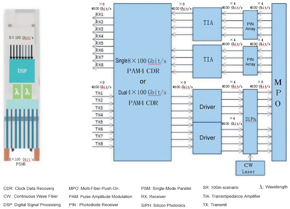
800G SR8 DML/EML Scheme: This approach employs 8 DSPs each operating at 100Gbit/s (potentially featuring analog clock data recovery units) along with DML/EML optoelectronic chips at the same wavelength. At both the transmitter and receiver ends, 8 optical fibers are utilized (utilizing PSM8 parallel single-mode 8-channel connections), and connectivity is achieved through 24-core or 16-core MPO connectors.
800G SR8 SiPh Scheme: In this approach, 8 SiPh (Silicon Photonics) Mach-Zehnder modulators (MZ) or Continuous Wave (CW) lasers are utilized. Silicon photonics is used as the transmission medium, with modulators and light sources separated. This enables a parallel multi-channel architecture sharing a single light source. Through proper insertion loss control, 1 to 2 light sources can support simultaneous parallel transmission for all 8 channels, providing a cost advantage.
For the 800Gbit/s 500m interconnect requirement, in the context of the 8x100Gbit/s SiPh scheme, there might be limitations in achieving cost reduction compared to the 400G DR4 (SiPh) solution. On the other hand, the 4x200Gbit/s scheme holds a potential cost advantage, although the yield of 100GBd devices still needs to be considered. In the early stages, the 8-channel parallel approach might still be seen as a feasible MSA (Multi-Source Agreement) solution.
As shown in Figure 5, the 800G DR4 (EML/SiPh) scheme employs 4x200Gbit/s DSPs. The optoelectronic chips are selected as 4xEML/SiPh, operating at the same wavelength. Due to bandwidth constraints, DML is not utilized. At both the transmission and reception ends, 4 optical fibers are employed (utilizing PSM4 parallel single-mode 4-channel connections), and connectivity is established using 12-core MPO connectors.
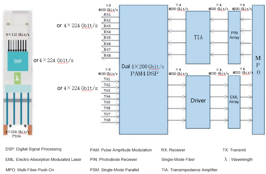
For the 800G 2km (FR) interconnect requirement, the PAM4 technology based on single-channel 200Gbit/s has emerged as the next-generation representative for intensity modulation and direct detection interconnects, forming the foundation for 4-channel 800G optical connections. When upgrading from 100Gbit/s to 200Gbit/s, the bit rate doubles, leading to a sensitivity drop of around 3dB. Hence, more robust forward error correction (FEC) codes are necessary to maintain higher receiver sensitivity (-5dBm).
The 800G FR4 EML scheme employs 4x200Gbit/s DSPs and CWDM4 EML optoelectronic chips. Wavelength-division multiplexing (WDM) is used at the transmitter and receiver ends, with each utilizing a single optical fiber (CWDM4). Connectivity is established using dual LC connectors, as depicted in Figure 6.
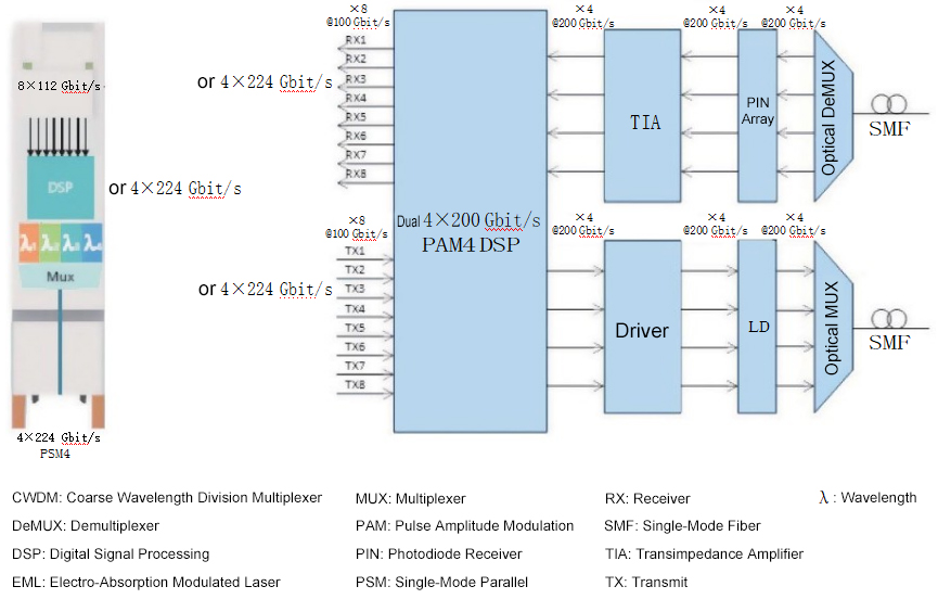
For the 800G 10km interconnect requirement, considering the challenges posed by dispersion limits, the industry has put forth four potential solutions: 800G LWDM8/nLWDM8, 800G LWDM4/nLWDM4, 800Gbit/s Self-Homodyne Detection (SHD) coherent, and 800G coherent solutions.
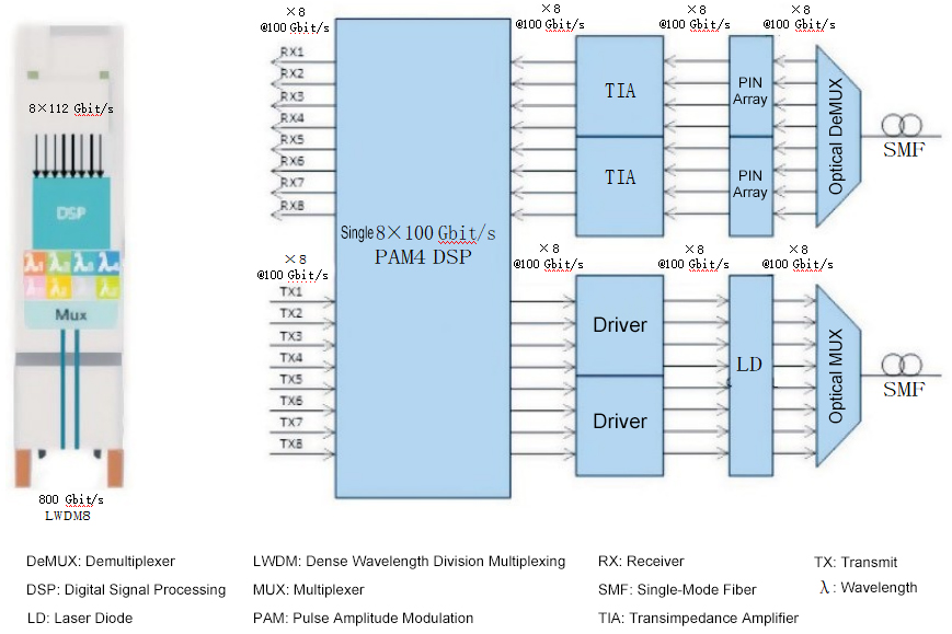
As illustrated in Figure 7, the 800G LR8 scheme employs 8x100Gbit/s DSPs and LWDM8 EML optoelectronic chips. At both the transmitter and receiver ends, wavelength-division multiplexing (WDM) is utilized, with each employing a single optical fiber (LWDM8). Connectivity is established using dual LC connectors.
The 800G LR4 scheme primarily employs 4x200Gbit/s DSPs and 4xEML LWDM4 wavelengths. The receiver side utilizes 200Gbit/s PAM4 waveguide avalanche photodiodes (APDs), as depicted in Figure 8. At both the transmitter and receiver ends, wavelength-division multiplexing (WDM) is used, with each end employing a single optical fiber(LWDM4). Connectivity is established using dual LC connectors.
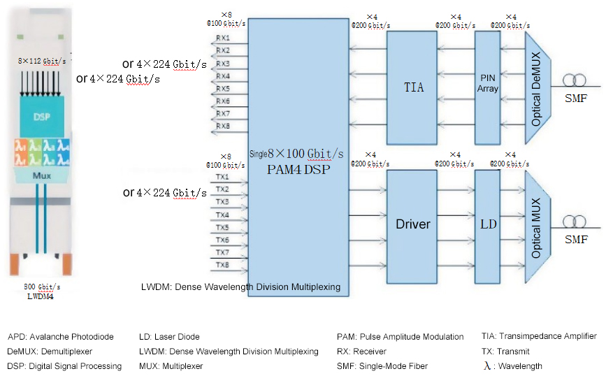
In the selection of a suitable wavelength scheme, there are currently two options: LWDM4 (800GHz wavelength spacing) and nLWDM4 (400GHz wavelength spacing). The nLWDM4 scheme offers advantages of lower dispersion cost, reduced DSP power consumption, and lower complexity. However, it requires the development of new EML (Electro-Absorption Modulated Laser) chips.
For the 800G 40km/80km interconnect requirements, the industry has adopted the 800Gbit/s coherent solution. This approach utilizes dedicated coherent DSPs, 128Gbd IC-TROSAs (Integrated Coherent Transmitter and Receiver Optical Sub-Assemblies), and connectivity is established using dual LC connectors.
The development trends of 800Gbit/s technology encompass the following three aspects:
(1)Migration to Single Mode Fiber: Due to the bandwidth limitations of multi-mode fiber, the distance for transmitting 100Gbit/s PAM4 signals using VCSELs over multi-mode fiber is confined to within 50m. Even with the utilization of OM5 fiber, system costs would increase. In the future, the adoption of single mode fiber interfaces will become an inevitable trend, which will have a positive impact SiPh (Silicon Photonics) technology.
(2)Rise of 200Gbit/s Single-Wavelength: While the development of 112 Gbd EML (Electroabsorption Modulated Laser) technology has progressed rapidly and prototypes have even been realized, the available bandwidth of 55 GHz falls slightly short. The potential of SiPh modulators operating at the 200Gbit/s PAM4 data rate level for a single wavelength, coupled with the promising application prospects of silicon-based thin-film lithium niobate technology, is poised to become a driving force in this direction.
(3)Coherent Technology Penetration: As transmission rates continue to increase, coherent technology will further extend its application to shorter transmission distances such as 40km, 20km, and 10km. Simultaneously, efforts are being made to enhance the reach of non-coherent technologies for longer distances. Consequently, these two technological approaches will intersect across various applications.
Competition between the two approaches will be influenced by factors such as cost per bit. Coherent solutions, despite their more complex devices, possess cost competitiveness comparable to PAM4 due to the requirement for only one laser, modulators, and receiver. On the other hand, PAM4 demands four individual lasers, modulators, and receivers, albeit simpler ones.
Although these devices might become more complex at 800Gbit/s, they are poised to rapidly reduce the overall system cost, maintaining PAM4’s competitive edge. Overall, the competition between coherent technology and PAM4 transmission has already begun, and the future outcome will require time to prove.
Additionally, the early-stage electrical interfaces for 800 optical modules encompass 8x100Gbit/s configurations. The optical interfaces include three options: 8x100G PAM4, 4x200G PAM4, and 128Gbd DP-16QAM coherent. Table 1 outlines the projected application scenarios for 800G optical modules.

Table 1: Predicted Application Scenarios for 800G Optical Modules
The migration to single mode supports wider coverage of 100m SR scenarios for the 800Gbit/s SiPh solution. Employing a common platform for both 800G SR8 and DR8, along with selective shipping based on specifications, aids in cost reduction. Moreover, SiPh optical modules might find breakthrough opportunities in the non-coherent domain.
The industry chain for 100G optical modules is diverse, but the industry chain for 200G modules is likely to be more concentrated, including both EML and MZ solutions. The single-wavelength 200Gbit/s optical interface will be used in 800Gbit/s and 1.6Tbit/s scenarios. The supply of 200Gbit/s PAM4 EML is limited, with insufficient bandwidth. Whereas 200Gbit/s PAM4 SiPh holds competitive advantages in terms of performance, cost, and industry chain diversity.
When the switching chip rate reaches 51.2Tbit/s, it will trigger demand for 800G optical modules. As the switching chip rate further increases to 102.4Tbit/s, the demand of both 800G and 1.6T optical modules will rise. Based on trends in switching chip evolution, market demand, and technological maturity, it is projected that 800G optical modules will enter the market around 2022. They are expected to achieve widespread adoption by around 2025. In the early stages, the 8x100Gbit/s solution will be the primary choice, facilitating a smooth transition from 400Gbit/s to 800Gbit/s.
When the single-channel electrical interface rate matches the optical interface rate, the architecture of optical modules will reach an optimal state, resulting in advantages such as low power consumption and low cost. The 4x200Gbit/s architecture is considered the ideal choice for 800G optical modules and will also serve as the foundation for 1.6T optical modules. However, as the frequency increases, the high-frequency signal integrity within the internal packaging might be compromised. As a result, cost considerations might come into play for 200Gbit/s per wavelength optical modules in terms of optoelectronic integration.
Furthermore, due to the increased baud rate, 200Gbit/s PAM4 DML (Distributed Feedback Laser) faces bandwidth limitations that affect its sensitivity for transmissions beyond 10km. As for the cost impact of high-bandwidth waveguide Avalanche Photodiodes (APDs) on medium to long-distance 800Gbit/s optical transmissions, it’s currently unclear.
根据具体的应用场景,可以采用不同的解决方案。对于超短距离,可以采用 8x100G 方案。短距离可能受益于 4x200G 方案。同时,对于中长距离,8x100G 方案可能仍然可行。然而,对于长距离传输,PAM4 色散和多径干扰等因素可能会发挥作用,使得 800G 相干解决方案可能更合适。