In today’s era where the demand for artificial intelligence and high-performance computing is growing exponentially, the network architecture of data centers is undergoing unprecedented transformation.
The network architecture of traditional cloud computing centers reveals significant limitations when confronting AI training tasks—when tens of thousands of GPUs need to collaborate in computation, the latency and power consumption associated with traditional electrical signal transmission become insurmountable bottlenecks. NVIDIA has observed that there is an essential difference between AI factories and traditional clouds: the former must support real-time communication for ultra-large-scale GPU clusters, with network density and bandwidth requirements growing exponentially.
This time, NVIDIA has achieved a breakthrough in the field of silicon photonics with its latest released NVIDIA Spectrum-X Photonics switch, which realizes an exponential leap in network performance through an optoelectronic integrated packaging optical architecture. This technology pioneers the world’s first 200Gb/s optoelectronic integrated packaging solution, highly integrating external digital signal processing units (DSP), 1.6Tb/s switching ASIC, and transceivers, thereby completely reconstructing the design logic of traditional pluggable switches.
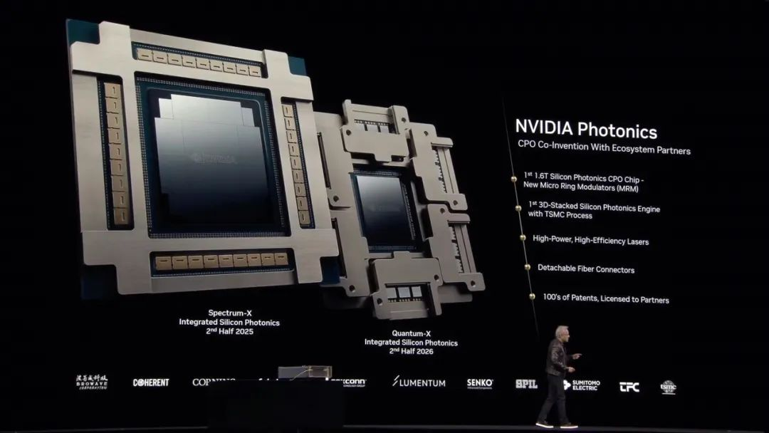
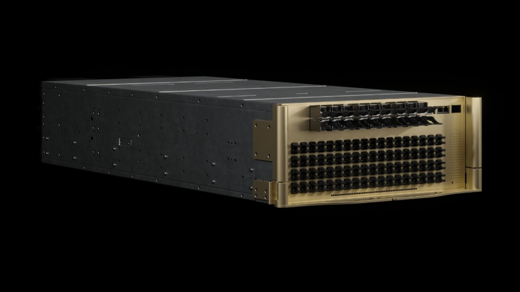
NVIDIA’s Co-Packaged Optics (CPO) switch is an advanced networking solution developed by NVIDIA to address the large-scale computing demands of the agentic AI era. It directly integrates silicon photonics technology into the switch ASIC (Application-Specific Integrated Circuit) package, replacing traditional pluggable optical transceivers to achieve efficient conversion and transmission of optical and electrical signals. This design significantly enhances the network’s power efficiency, bandwidth, and reliability, primarily applied in data center AI factories to support the interconnection of millions of GPUs.
Networks based on NVIDIA CPO can simplify management and design, while enhancing the performance of computing infrastructure. These advantages are crucial for achieving large-scale deployment of future million-GPU AI factories.
What is Silicon Photonics Integrated Packaging?
Silicon Photonics Integrated Packaging, also commonly known as Silicon Photonics Co-Packaged Optics (CPO), is an advanced optoelectronic integration technology. It tightly integrates silicon photonic devices (such as optical transceivers and optical engines) with electronic chips (such as ASICs, switch ICs, or CPUs) through advanced packaging processes, rather than using traditional pluggable optical module forms. This integration typically retains external optical port interfaces to achieve efficient conversion and transmission of optical and electrical signals.
Silicon Photonics Integrated Packaging technology is an evolution in hardware integration. By directly packaging silicon photonic transceivers with the switch IC, NVIDIA has achieved:
Reduced Power Consumption
Compared to traditional pluggable optical modules, Silicon Photonics Integrated Packaging can achieve a significant 3.5x reduction in power consumption. By eliminating power-hungry external DSP devices and shrinking signal paths from inches to millimeters, this breakthrough technology significantly improves energy efficiency. This denser and more sustainable AI infrastructure will drive faster system visibility and scalability to meet the demands of next-generation AI.
Reduce Component Count
Reducing the number of components means simplifying the manufacturing process and decreasing failure points. By directly integrating optical devices into the package, it lowers the complexity of procuring, assembling, and testing a large number of tiny components, which is a common challenge faced by traditional systems based on optical modules.
Enhance Performance
After integrating optical devices, the connections between the switch ASIC and optical transceivers will be designed, assembled, and tested at the IC package level, eliminating sources of signal attenuation and also removing the need for independent digital signal processors (DSPs), which often introduce latency and consume additional power.
Simplify Data Center Operations
Simplifying construction can accelerate deployment speed and streamline maintenance.
Main Advantages of Switches Based on NVIDIA Silicon Photonics Technology
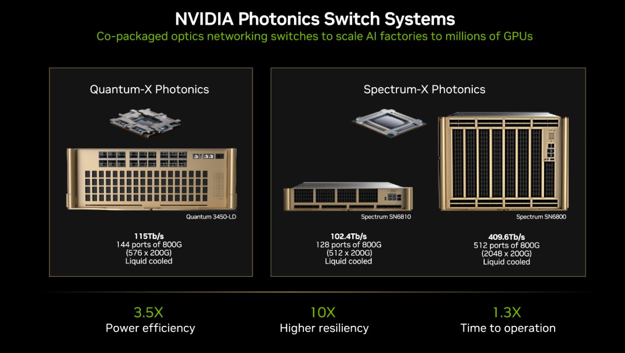
The NVIDIA silicon photonics network switch launched this time demonstrates the significant advantages of CPO technology. Compared to traditional methods, this solution reduces the number of lasers by a factor of 4, improves energy efficiency by up to 3.5 times, enhances signal integrity by up to 63 times, increases large-scale networking reliability by up to 10 times, and accelerates deployment speed by up to 1.3 times. These data indicate that CPO not only optimizes network performance but also reduces system complexity and long-term operation and maintenance costs.
Lower Power Consumption
The DSP used in traditional modules significantly increases power consumption. For example, a 1.6 Tbps optical module requires approximately 30 watts of power, with more than half consumed by the DSP.
By utilizing NVIDIA’s integrated silicon photonics technology, in the long term, the energy consumption of AI data centers can be reduced by a factor of 3.5 compared to those based on traditional optical modules.
Increase Network Uptime and Reliability
When traditional optical modules fail, it may require hours of manual intervention for troubleshooting and repair. In contrast, silicon photonics integrated packaging technology adopts a simpler design with fewer components, which can significantly reduce the probability of optical module failures. This integrated design can minimize downtime in AI data centers to a greater extent, enhance network reliability, and ensure the network remains fully operational, which is crucial for uninterrupted AI training and inference.
Lower Latency and Better Signal Integrity
NVIDIA’s silicon photonics technology directly integrates optical signal devices into the switch IC package, improving signal integrity by reducing the number of components and dramatically shortening signal paths. In traditional switch designs based on optical modules, signals need to be transmitted 14 to 16 inches through printed circuit boards or copper wires, thereby increasing the risk of signal interference. With silicon photonics technology, the signal path is less than 0.5 inches, greatly reducing this risk.
Switches based on optical modules also rely on DSPs (digital signal processors) to clear signal interference, which significantly increases latency. By directly integrating silicon photonics devices into the switch IC, this additional processing step is eliminated, thereby reducing latency and improving network efficiency, which is essential for high-speed AI workloads and modern data center performance.
Accelerate Deployment Speed
Compared to similar systems deployed using pluggable optical modules, after adopting silicon photonics integrated packaging technology, system installation becomes a simple “plug-and-play” process, with deployment speed increased by 1.3 times.
Easy On-Site Maintenance
This design places the most failure-prone component (i.e., the laser) in the OSFP module on the front panel of the switch, facilitating the plugging and unplugging of the external laser source (ELS). If a failure occurs, it can be quickly diagnosed and easily replaced.
In summary, NVIDIA’s Co-Packaged Optics (CPO) switches integrate photonic devices directly into the switch ASIC, delivering unprecedented gains in power efficiency, bandwidth, and network reliability. This breakthrough overcomes the limitations of traditional pluggable optical modules in terms of latency, power consumption, and signal integrity, laying a solid foundation for future AI factories with millions of interconnected GPUs. As the AI era accelerates, CPO is poised to become a key driver of data center network evolution, ushering in the next generation of high-performance computing infrastructure.
References
- NVIDIA Silicon Photonics
- NVIDIA Blog – Spectrum-X Co-Packaged Optics Networking Switches for AI Factories
- Image Credit: NVIDIA
Post Views: 6,079