Understanding Co-Packaged Optics: Revolutionizing Data Center Connectivity
June 24, 2025
As data centers scale to support cloud computing, artificial intelligence (AI), and high-performance computing (HPC), traditional electrical interconnects struggle to meet bandwidth and latency requirements. CPO offers a solution by reducing signal loss, improving power efficiency, and enabling denser connectivity. This makes it a critical enabler for next-generation networking, particularly in environments where performance and scalability are paramount.
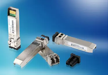
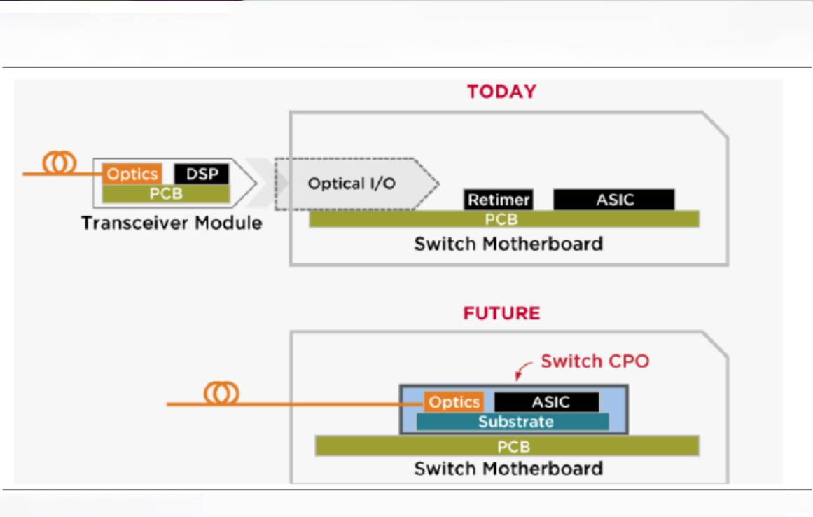
Co-packaged optics (CPO) represents a transformative approach in optical networking, where optical and electronic components are tightly integrated into a single package, typically on the same substrate as the chip. Unlike traditional pluggable optics that rely on separate modules connected through copper traces, CPO integrates optical transceivers directly next to processing chips like ASICs or GPUs. This co-packaged approach enables high-speed, low-latency data transmission while reducing power consumption and physical footprint. This technology addresses the escalating demands of modern data centers for higher bandwidth, reduced power consumption, and compact designs.
Co-Packaged Optics (CPO) technology further shortens the electrical interconnect length between the optical signal input and the processing units. By increasing the interconnect density between optical modules and ASIC chips while reducing power consumption, CPO provides a critical technological solution for addressing the challenges of high-speed, large-volume data transmission in future big data processing applications.
Image source: Broadcom official website
Key Advantages of Co-Packaged Optics (CPO) Technology
CPO (Co-Packaged Optics) technology offers significant benefits by tightly integrating optical components with switching ASICs. The core advantages of Co-Packaged Optics (CPO) technology are mainly reflected in the following aspects:
Low Power Consumption & High Efficiency
CPO significantly reduces power consumption by minimizing the electrical trace length between the optical module and the ASIC. This shorter signal path reduces SerDes losses and lowers the need for power-hungry signal compensation techniques. Combined with optimized electrical interconnects and signal processing, CPO offers far better energy efficiency than traditional pluggable optics.
High Bandwidth & Signal Integrity
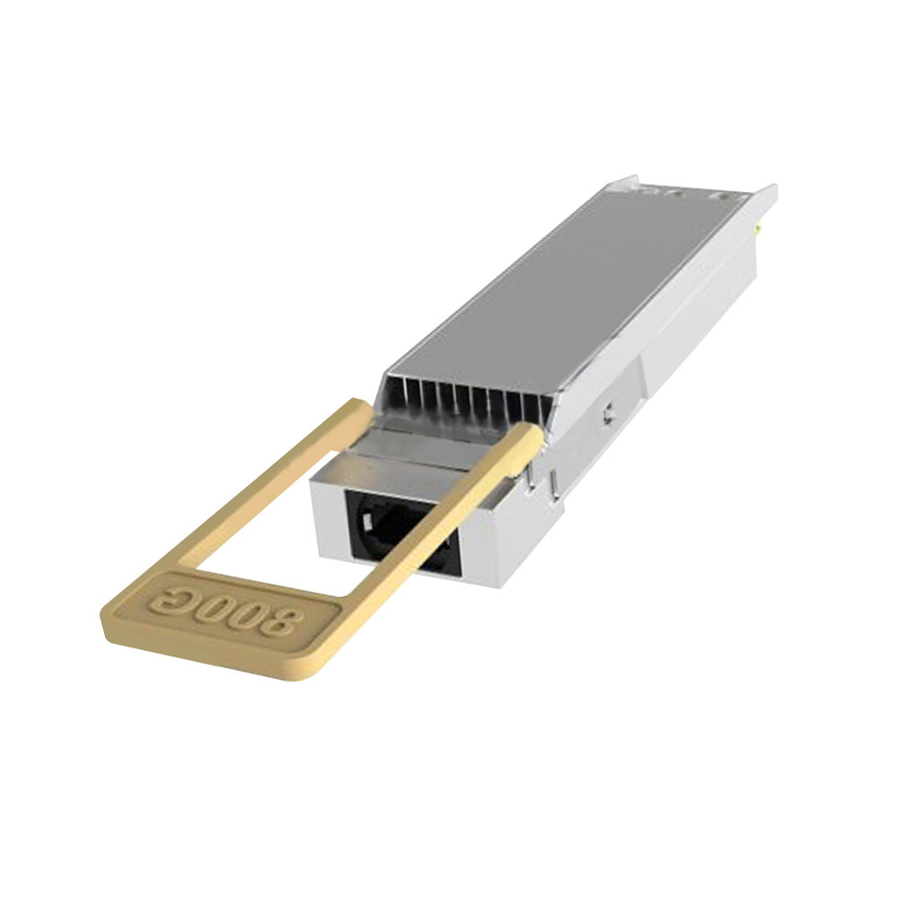
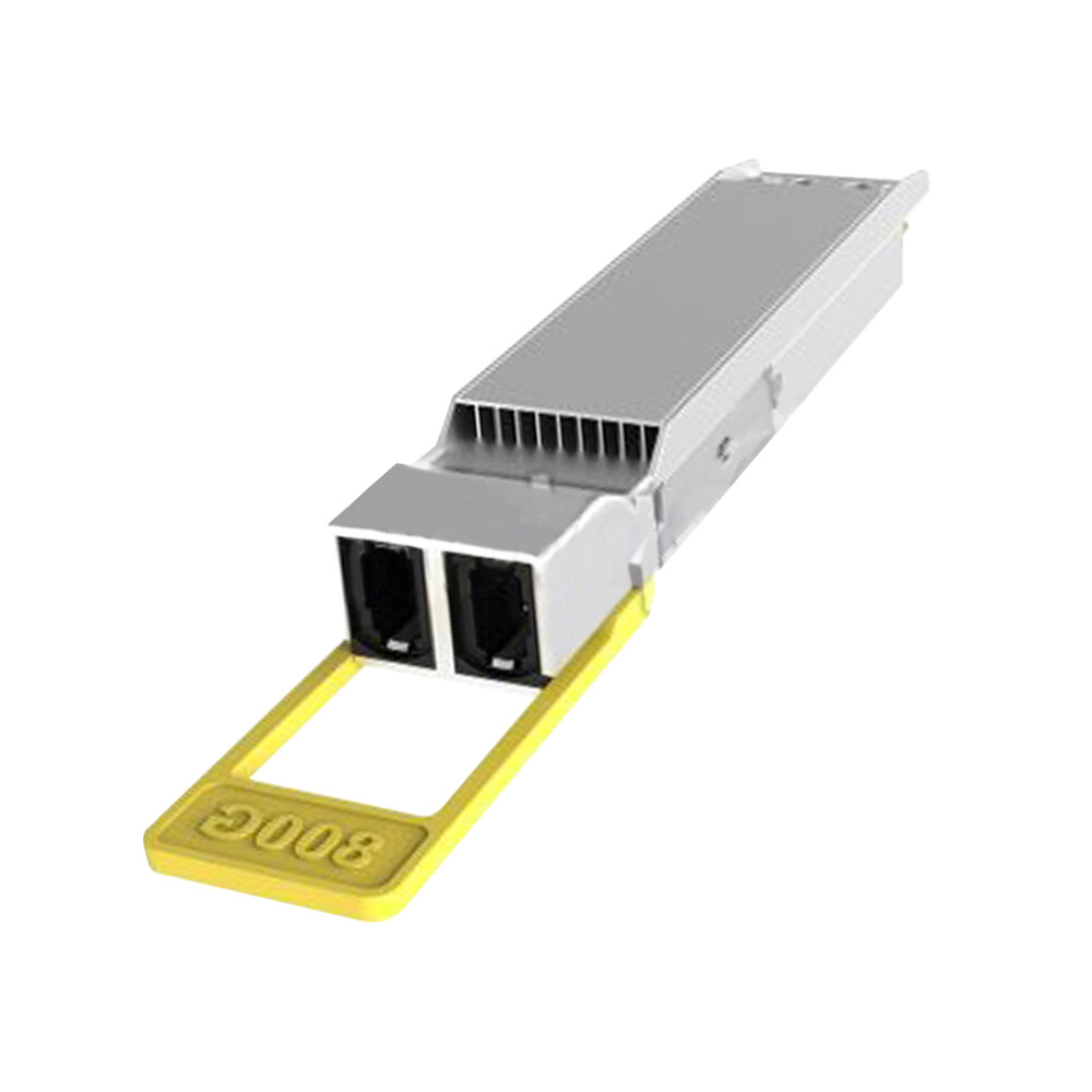
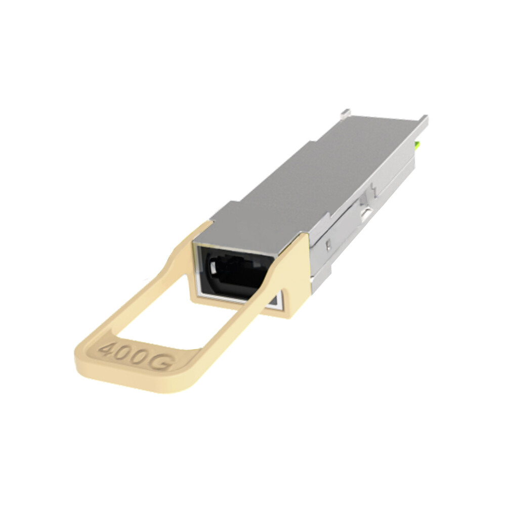
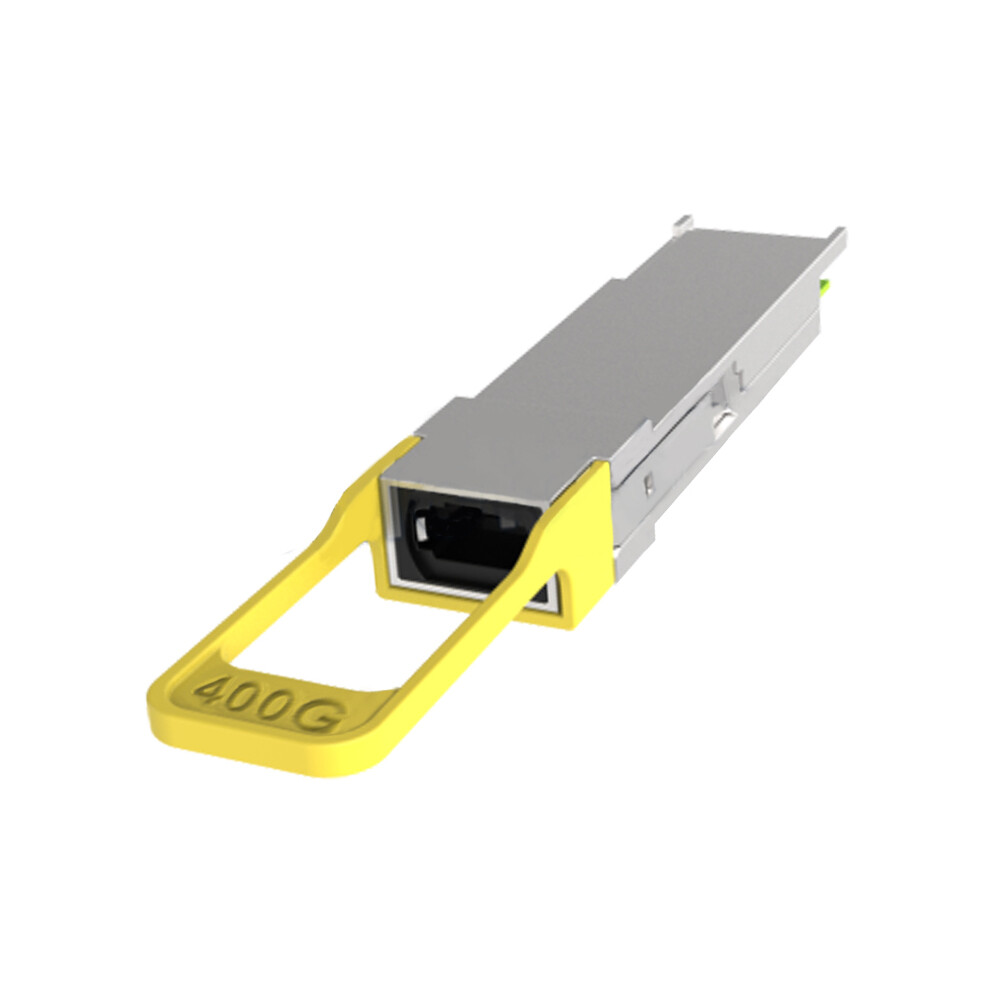
With support for high-speed configurations such as 400G, 800G, and 1.6T, CPO provides the bandwidth necessary for next-generation switches and data center workloads. The reduced electrical path length also minimizes signal degradation and latency, resulting in superior signal integrity and more reliable high-speed data transmission.
Compact Size & High Integration
CPO achieves a compact form factor by co-packaging optical and electronic components in a single, space-saving module. This high level of integration significantly reduces the physical footprint of interconnects and enables higher port density in switch systems—ideal for space-constrained, high-density data center environments.
Cost Optimization
By simplifying the system architecture and reducing the number of discrete components, CPO can lower both manufacturing and deployment costs. The integrated design also facilitates automated production, improving manufacturing yield and efficiency, which helps reduce the total cost of ownership over time.
System Reliability
CPO enhances system reliability by minimizing physical connection points that often become sources of failure. The integrated architecture not only improves overall system stability but also simplifies maintenance. Modular design features allow easier replacement and servicing, reducing downtime and operational risk.
Thermal Management & Scalability
The dense integration of optical and electronic components in CPO modules demands advanced thermal solutions. CPO systems often utilize liquid or microfluidic cooling to manage heat effectively under high-performance loads. Additionally, CPO’s modular and forward-compatible architecture supports future scaling, making it well-suited for evolving workloads in AI, cloud computing, and high-performance computing.
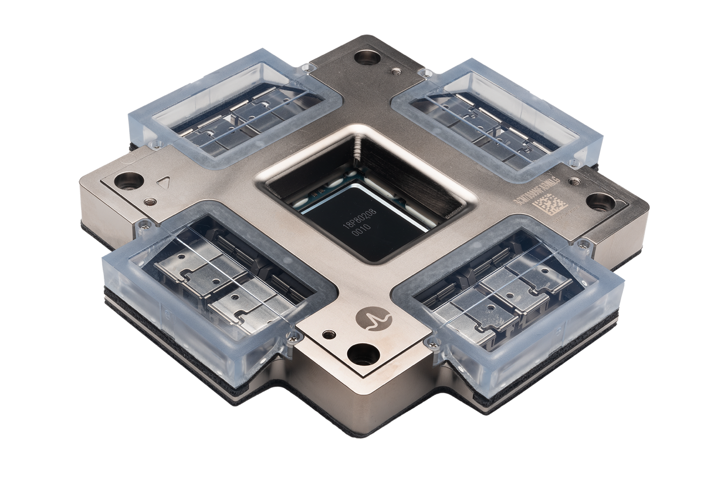
Key Innovations in Co-Packaged Optics
Integration of Optical and Electronic Components
CPO’s core innovation lies in its ability to combine photonic and electronic elements within a single package. This integration leverages advanced packaging techniques, such as 2.5D and 3D stacking, to place optical transceivers alongside compute chips, minimizing signal paths and enhancing performance.
Elimination of High-Loss Copper Traces
Copper traces in traditional setups contribute to signal loss and power inefficiency, especially at high data rates. CPO replaces these with optical interconnects, which offer lower attenuation and support longer-distance communication without significant signal degradation.
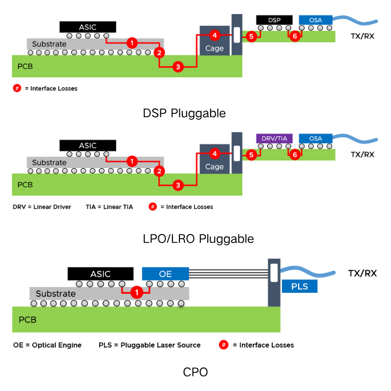
Reduction of DSP Usage
Digital signal processors (DSPs) are often used in pluggable optics to compensate for signal distortions, but they consume significant power. CPO’s direct optical integration reduces the need for DSPs, streamlining data transmission and lowering energy requirements.
Linear-Drive Pluggable Optics (LPO)
Linear-drive pluggable optics (LPO) is an emerging technology complementary to CPO, offering simplified signal processing for short-reach applications. While not fully co-packaged, LPO shares CPO’s goal of reducing power and complexity, making it a stepping stone toward broader CPO adoption.
Image source: Broadcom official website
Comparison Between CPO and Pluggable Optical Modules
Co-Packaged Optics (CPO) technology differs significantly from traditional pluggable optical modules across several key dimensions, including power consumption, bandwidth, form factor, integration, cost efficiency, reliability, thermal performance, and system flexibility.
Low Power Consumption
CPO reduces power consumption by shortening the electrical signal transmission path between the switch ASIC and the optical engine, minimizing SerDes losses. This results in more than 50% lower power compared to pluggable optics. For example, an 800G CPO module typically consumes around 5W, whereas a pluggable module may reach 16W.
However, when using an external laser source (ELS), coupling losses of 1.8–3 dB can increase laser power consumption by 50% to 100%. In contrast, pluggable modules rely on DSPs for signal compensation, resulting in higher power consumption (typically 12–16W for 800G). The emerging Linear Pluggable Optics (LPO) approach eliminates DSPs to reduce power consumption to below 4W.
High Bandwidth
CPO supports much higher channel density—for instance, 1.6T CPO modules can incorporate 16×100G lanes, enabling compatibility with 51.2T or even 102.4T switches. This increases bandwidth density by up to 8×. Silicon photonics allows single-wavelength 200G transmission and targets up to 3.2Tbps in the future. Pluggable modules currently offer up to 800G (8×100G), while 1.6T solutions require larger OSFP-XD form factors. However, higher speeds above 224G SerDes face signal integrity challenges due to PCB trace losses.
Compact Size
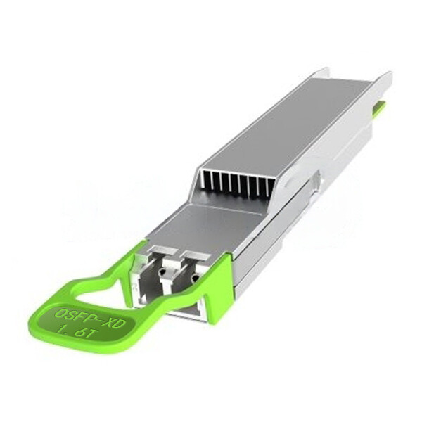
CPO co-packages the optical engine with the ASIC, reducing overall size by more than 50%. Some modules, such as Intel’s CPO solution, are as small as a coin. Pluggable modules require separate housings and connectors (e.g., QSFP-DD), making them bulkier. Newer formats like OSFP-XD offer improved density but still cannot match the compactness of CPO.
High Integration
CPO leverages silicon photonics and 3D packaging technologies to achieve tight optoelectronic integration, as seen in designs from Broadcom. However, this level of integration requires advanced semiconductor processes (e.g., 3nm DSPs). In contrast, pluggable modules use modular architectures with separate optical and electrical components, allowing greater flexibility in design and production, and compatibility with existing supply chains.
Cost Efficiency
CPO requires high initial R&D investment, including custom ASICs and optical engines. However, long-term savings of up to 30% are possible by reducing the number of optical fibers and connectors. Challenges remain in manufacturing yield, particularly with silicon photonic coupling losses. Pluggable modules benefit from a mature supply chain and relatively low unit costs. However, their higher power consumption contributes to increased total cost of ownership (TCO) in large-scale deployments.
Reliability
A key concern with CPO is that a laser failure can affect the entire board, requiring redundant laser designs to ensure uptime. IBM, for example, uses backup lasers to reduce failure rates by up to 1000×. In contrast, pluggable modules support hot-swapping and are easier to replace when faults occur. With typical failure rates around 2%, they offer low maintenance costs and operational flexibility.
Thermal Performance
Due to high integration, CPO modules exhibit concentrated heat density, often requiring advanced cooling solutions like liquid cooling or microfluidics, as seen in NVIDIA’s Spectrum-X architecture. Pluggable modules come with independent heat dissipation structures (e.g., OSFP with heat sinks). While this works for most current modules, higher power designs (e.g., 1.6T) still require active or forced cooling.
Flexibility
CPO systems are typically tied to specific ASIC vendors (e.g., Broadcom Bailly), meaning system upgrades often require replacing the entire board, which limits ecosystem openness. Pluggable modules, on the other hand, follow open standards (e.g., QSFP-DD MSA), allowing multi-vendor compatibility and smoother upgrade paths, such as transitioning from 400G to 800G.
Traditional pluggable optics rely on external modules connected via electrical traces, which introduce signal degradation and power inefficiencies. In contrast, CPO integrates optical transceivers directly into the chip package, reducing signal loss and enabling higher data rates. While pluggable optics remain modular and easier to replace, CPO offers superior performance for high-density, high-speed applications.
Applications and Use Cases
Data Center Networking
CPO is poised to revolutionize data center networking by enabling ultra-high-speed connections between servers, switches, and storage systems. Its compact design supports dense rack configurations, making it ideal for hyperscale data centers.
AI and High-Performance Computing (HPC)
AI and HPC workloads require massive data throughput and low latency. CPO’s ability to deliver high-bandwidth, low-power connectivity makes it a critical technology for training large-scale AI models and running complex simulations.
Cloud and Enterprise Solutions
Cloud providers and enterprises benefit from CPO’s scalability and efficiency, enabling them to handle growing data demands while reducing operational costs. CPO supports the transition to optical I/O, paving the way for future-proof infrastructure.
Future of Co-Packaged Optics
The relentless demand for lower per-bit costs and reduced power consumption continues to drive the advancement of Co-Packaged Optics (CPO) technology. According to Cisco data, between 2010 and 2022, global data center network switching bandwidth surged by 80 times, while the power consumption of switching chips increased approximately 8-fold.
Over the same period, optical module power consumption rose by 26 times, and the power consumption of serializer/deserializer (SerDes) in switching chips grew by 25 times.
Recently, Broadcom officially launched its third-generation silicon photonics co-packaged optics (CPO) technology, capable of achieving ultra-high-speed data transmission at 200G per lane—doubling the bandwidth of traditional copper-based solutions. This breakthrough significantly reduces power consumption and signal interference, positioning it as a benchmark for next-generation interconnects targeting hyperscale data centers and AI workloads.
Data source: Broadcom official website, GF Securities Development Research Center
Potential for Data Center Transformation
CPO has the potential to redefine data center architecture by enabling denser, more efficient, and higher-performing networks. As adoption grows, CPO could reduce the physical footprint of data centers while supporting unprecedented data growth.
(1)Scalability for Future Network Demands
With data traffic projected to double every few years, CPO’s scalability ensures it can meet future demands. Its ability to support terabit-scale connectivity positions it as a cornerstone of next-generation networking.
(2)Cost and Power Savings
By reducing power consumption and enabling compact designs, CPO offers significant cost savings over time. These benefits make it an attractive option for data center operators seeking to optimize operational expenses.
Challenges and Considerations
(1)Technical Design Complexities
Designing CPO systems involves managing thermal, mechanical, and optical challenges. Engineers must balance performance with manufacturability, requiring advanced tools and expertise.
(2)Testing and Yield Challenges
Since optical chips are directly integrated with electrical chips through advanced packaging technologies, this presents numerous challenges for yield and testing. Moreover, optical and electrical components are built on different manufacturing processes, which leads to different testing requirements. The co-packaged optical devices have a high channel density, which further complicates the testing process.
(3)Adoption Barriers
Despite its advantages, CPO faces adoption challenges, including high development costs, complex manufacturing processes, and the need for new supply chain models. Overcoming these barriers requires industry-wide collaboration.
(4)Multi-Vendor Business Models
CPO’s success depends on interoperability across vendors. Multi-vendor ecosystems require standardized interfaces and robust testing to ensure compatibility and reliability.
Conclusion
Co-Packaged Optics (CPO) technology is becoming a key innovation in data centers and high-performance computing, thanks to its low power consumption, high bandwidth, and high integration. As the technology matures and industry collaboration increases, CPO is expected to be widely adopted, revolutionizing data center architecture and providing a strong foundation for growing network demands.
Although challenges like high development costs and design complexity remain, CPO will play a bigger role in next-generation networks as standardization progresses.
Frequently Asked Questions (FAQ)
Q: How does CPO differ from traditional pluggable optics?
A: CPO integrates optical transceivers directly into the chip package, reducing signal loss and power consumption compared to pluggable optics, which use external modules and copper traces.
Q: What are the main benefits of CPO for data centers?
A: CPO offers higher bandwidth density, lower latency, and reduced power consumption, enabling more efficient and scalable data center networks.
Q: How are industry standards shaping CPO development?
A: Organizations like IEEE and OIF are defining interoperable CPO standards, ensuring compatibility and accelerating adoption across the industry.
Q: What are the current limitations of adopting CPO technology?
A: Challenges include high development costs, complex manufacturing, and the need for standardized multi-vendor ecosystems to ensure broad adoption.