The rapid development of artificial intelligence, 5G, the Internet of Things, and big data is accelerating the evolution of computing architectures. According to IDC, global data volume is expected to reach 213.6 ZB in 2025 and more than double to 527.5 ZB by 2029. This explosive data growth is placing unprecedented pressure on data centers in terms of bandwidth, latency, and energy consumption.
At the same time, traditional optoelectronic technologies based on III-V compound materials are approaching their physical and cost limits. As pluggable optical modules advance toward 800G and 1.6T, challenges related to power density, form-factor constraints, and signal integrity are becoming increasingly prominent, limiting further system scalability.
Against this backdrop, silicon photonics has emerged as a new solution. By combining the maturity of silicon manufacturing with the high bandwidth and low-power advantages of photonic technologies, silicon photonics has the potential to overcome power and interconnect bottlenecks, becoming a critical foundation for next-generation computing systems.
Principles and Advantages of Silicon Photonics
Silicon photonics is a technology that integrates optical and electronic components on a silicon substrate. By leveraging mature CMOS manufacturing processes, silicon photonics enables the generation, modulation, transmission, and detection of optical signals on a single chip, forming the foundation for high-speed optoelectronic interconnects.
Its operation is based on several key building blocks:
Light Source Coupling:
Because silicon itself is not an efficient light emitter, silicon photonic systems typically rely on external laser sources, such as EML or DFB lasers. Light is introduced into the silicon photonic chip through hybrid integration or optical coupling techniques.
Optical Modulation:
Within silicon waveguides, modulators based on the plasma dispersion effect—most commonly Mach–Zehnder modulators (MZMs)—are used to encode high-speed electrical signals onto optical carriers, enabling efficient electrical-to-optical conversion.
Optical Transmission and Multiplexing:
Optical signals propagate through silicon waveguides and can be multiplexed using on-chip wavelength-division multiplexing (WDM) devices. This allows multiple wavelengths to be transmitted in parallel, significantly increasing bandwidth density.
Optical Detection:
At the receiver side, integrated germanium (Ge) photodetectors convert incoming optical signals back into electrical signals, enabling high-speed data reception.
Core Advantages of Silicon Photonics
-
High Integration for Increased Bandwidth Density
Silicon photonics enables the integration of modulators, multiplexers/demultiplexers, and photodetectors on a single chip, significantly reducing module size. This high level of integration is well suited to the high port-density requirements of 400G, 800G, and next-generation optical modules.
-
CMOS Compatibility and Cost Efficiency
Silicon photonic devices can be manufactured using mature CMOS processes, enabling high-volume production. Compared with traditional III-V–based optical devices, silicon photonics offers greater long-term cost reduction potential, making it attractive for large-scale data center deployments.
-
Lower Power Consumption for High-Speed Interconnects
By shortening optoelectronic interconnect paths and minimizing electrical signal transmission distances, silicon photonics helps reduce overall system power consumption. This advantage is particularly critical for AI data centers and HPC environments, where energy efficiency is a primary concern.
-
Native Support for Wavelength Division Multiplexing (WDM)
Silicon photonics excels in waveguide and optical component integration, enabling high-density on-chip WDM. This makes it a key enabling technology for multi-wavelength solutions such as FR4, LR4, and ZR.
-
Easy Co-Packaging with High-Speed Electronic Chips
Silicon photonic chips can be co-packaged or closely integrated with switch ASICs, DSPs, or SerDes. This capability provides a strong foundation for future ultra-high-speed, low-latency optical interconnect architectures, including CPO.
Silicon Photonics: The Key Technology Pathway to Enabling CPO
As switch chip speeds continue to increase, the traditional pluggable optical module architecture is gradually approaching physical limits in terms of power consumption, bandwidth density, and signal integrity. Co-Packaged Optics (CPO) is emerging as a major evolution direction for next-generation data center networks, and silicon photonics is the core enabling technology that makes CPO commercially viable.
From Pluggable to Co-Packaged: The Inevitable Choice in Architecture Evolution
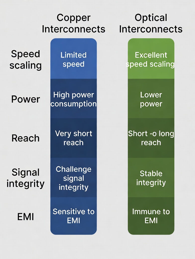
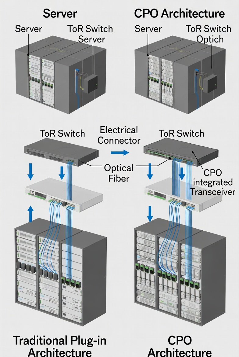
In conventional network architectures, high-speed electrical signals between the switch ASIC and optical modules are transmitted via PCB traces and connectors. As SerDes rates advance to 112G and even 224G, the issues of increased power consumption, signal attenuation, and rising system complexity caused by electrical interconnects become increasingly severe.
The core idea of CPO is to bring the optical-electrical conversion as close as possible to the switch chip — performing the conversion from electrical to optical signals inside the package itself. This dramatically shortens the electrical interconnect distance, significantly reduces system power consumption, and greatly improves overall bandwidth density.
How Silicon Photonics Enables the CPO Architecture
Silicon photonics technology is based on mature CMOS processes, allowing highly integrated modulators, waveguides, multiplexers/demultiplexers, and photodetectors to be fabricated on a single chip. This high level of integration makes it particularly well-suited for close-proximity — or even co-packaged — deployment with switch ASICs.
In a CPO architecture, the high-speed SerDes of the switch chip can directly drive silicon photonic modulators through millimeter-scale electrical connections. This dramatically reduces the signal loss and power consumption caused by traditional long PCB traces. At the same time, the silicon photonic chip can implement high-density wavelength division multiplexing (WDM) on-chip, delivering Tbps-level optical bandwidth output within a very limited physical space.
External Laser Source and System-Level Optimization
Due to the inherent inability of silicon materials to efficiently emit light, CPO systems typically adopt an External Laser Source (ELS) to provide a stable optical source for the silicon photonic chip. This design not only helps reduce the thermal load inside the package, but also improves system reliability and long-term maintainability.
After modulation and wavelength division multiplexing are performed on the silicon photonic chip, the optical signal is then output through optical fibers, enabling efficient connection from the switch chip all the way to the network link.
Key Foundation for Driving Ultra-High-Speed Interconnects
Leveraging silicon photonics technology, CPO can support higher SerDes rates and higher port bandwidth density at significantly lower power consumption, laying the foundation for network architectures at 800G, 1.6T, and even faster speeds. Although challenges remain in packaging complexity, thermal management, and operational maintenance models, in ultra-scale AI data centers and HPC scenarios, the silicon photonics-driven CPO architecture is already regarded as a critical direction for the next phase of network evolution.
Application Value and Growth Potential of CPO in Scale-up Architectures
As AI computing paradigms gradually shift from pure scale-out (horizontal scaling) to scale-up (increasing compute power per single node), intra-server and intra-rack interconnects are becoming the new performance bottlenecks. GPUs, CPUs, and various AI accelerators require ultra-high-frequency data exchange over extremely short distances, imposing far stricter requirements on bandwidth, latency, and energy efficiency than traditional data center networks.
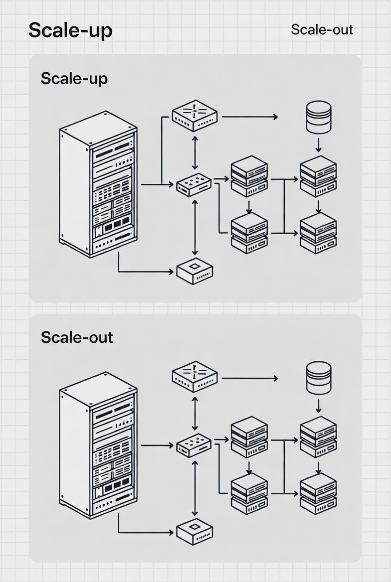
Against this backdrop, the synergistic development of silicon photonics and CPO (Co-Packaged Optics) is opening up new market opportunities for scale-up architectures. Unlike pluggable optical modules designed for inter-rack or data-center-level interconnects, CPO (including variants such as NPO and LPO) is far better suited for short-distance, high-speed interconnect scenarios within racks, on boards, and chip-to-chip. By moving the optical-electrical conversion closer to the chip or package level, the system can achieve significantly higher bandwidth and much lower power consumption over dramatically shorter electrical interconnect distances.
From a system design perspective, CPO offers clear advantages. On one hand, its performance evolution path can be highly aligned with compute chips, allowing chip vendors to independently define interconnect bandwidth and topology, thereby further expanding single-node compute scale. On the other hand, ultra-short-distance optical interconnects effectively circumvent the signal integrity and power consumption bottlenecks faced by high-speed copper interconnects at advanced rates, providing a sustainable solution for 112G, 224G, and even higher-speed interconnects.
In summary, CPO is fundamentally a short-reach, low-power, high-bandwidth optical communication solution. As AI servers continue to evolve toward higher integration and greater energy efficiency, silicon photonics-driven CPO is expected to achieve large-scale commercial deployment first in scale-up architectures, and to become a key foundational component in future high-performance AI computing platforms.
Conclusion
As interconnect bandwidth and energy efficiency become critical constraints for AI systems, silicon photonics and CPO offer a clear path forward. By reducing electrical interconnect distances and improving bandwidth density, they enable scalable, low-power architectures suited for next-generation AI and high-performance computing platforms.
Post Views: 10,945