In the wave of rapid development of artificial intelligence, the performance improvement of computing chips is undoubtedly the core driving force. However, as AI application scenarios become increasingly complex, the importance of network connectivity and data processing capabilities is gradually becoming prominent. At the GTC conference held on March 18, 2025, NVIDIA, with its forward-looking technological vision, launched two innovative achievements: Co-Packaged Optics (CPO) technology and the NVIDIA AI Data Platform.
This not only marks a new breakthrough for NVIDIA in the field of AI infrastructure but also provides strong technical support for building million-GPU-level AI factories and enterprise intelligent transformation, opening a new chapter in the AI ecosystem.
IDC predicts that 2025–2026 will be a critical window for pilot deployments of CPO, with hyperscale data centers taking the lead in validating its value. CPO technology not only meets the exponentially growing bandwidth demands of the AI era but also drives data centers toward all-optical networks, becoming a cornerstone for supporting AI adoption and digital transformation.
This article will discuss the advantages of CPO technology and why its development is essential.
Overview of Co-Packaged Optics (CPO) Technology
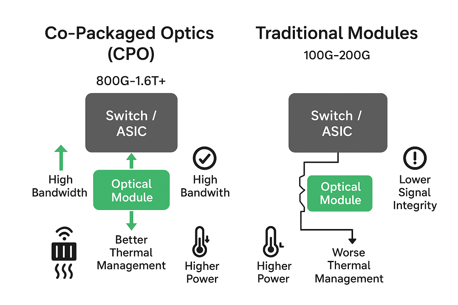
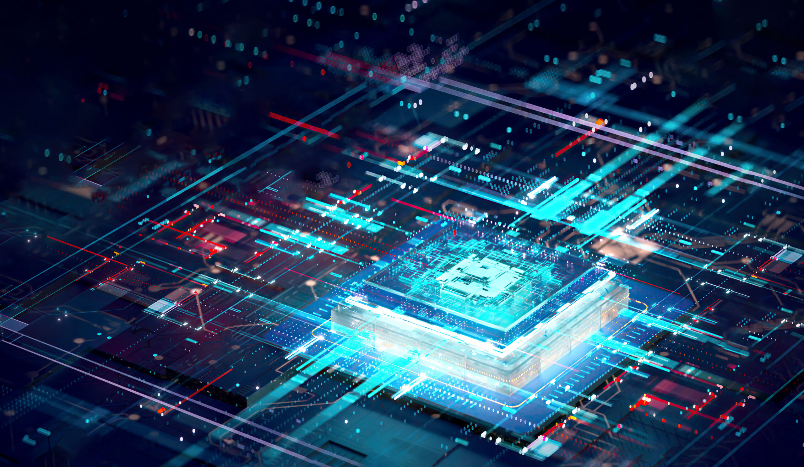
Co-Packaged Optics (CPO) is an advanced integration technology that tightly packages optical components (such as Photonic Integrated Circuits, PIC) and electronic chips (such as ASIC switch chips) on the same substrate, rather than using traditional external pluggable optical modules. This design significantly shortens the electro-optical signal conversion path, reduces intermediate electrical interfaces, thereby lowering power consumption and latency.
CPO is a key bridge for data center networks to evolve towards all-optical, driving the transition from electrically dominated interconnects to optically dominated networks, ultimately achieving more data transmission and processing in optical form, reducing the number of electro-optical conversions.
Traditional network architectures based on electrical signal transmission face severe challenges in terms of signal loss, power consumption, and scalability. The emergence of CPO technology fundamentally transforms data transmission by directly integrating optical components—such as lasers, optical modulators, and photodetectors—with core computing chips.
Compared with conventional solutions, CPO replaces electrical signals with optical signals, drastically reducing signal loss between the chip and the optical interface. This not only enables an exponential increase in data throughput but also significantly lowers energy consumption. Such a technological breakthrough provides a solid foundation for the large-scale deployment of AI factories.
Core Drivers for Developing CPO
The main purpose of developing CPO is to break through the bottlenecks of traditional electrical interface packaging in terms of bandwidth, power consumption, signal integrity, and other aspects, to address the rapidly growing demands in the fields of artificial intelligence (AI) and high-performance computing, and to drive the optimization and upgrading of data center network architectures. This technology directly integrates optical devices into the chip package, replacing traditional pluggable optical modules, thereby resolving the bottlenecks of traditional networks in AI training and inference tasks. Here are several key reasons:
1. Reducing Power Consumption and Improving Energy Efficiency
This is the core demand driven by AI and high-performance computing, and it is the most direct and urgent driving force for developing CPO.
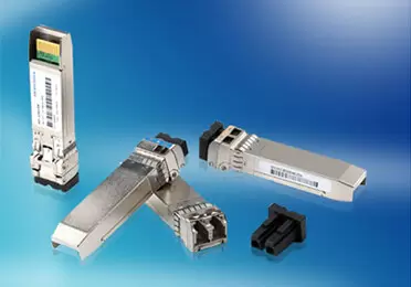
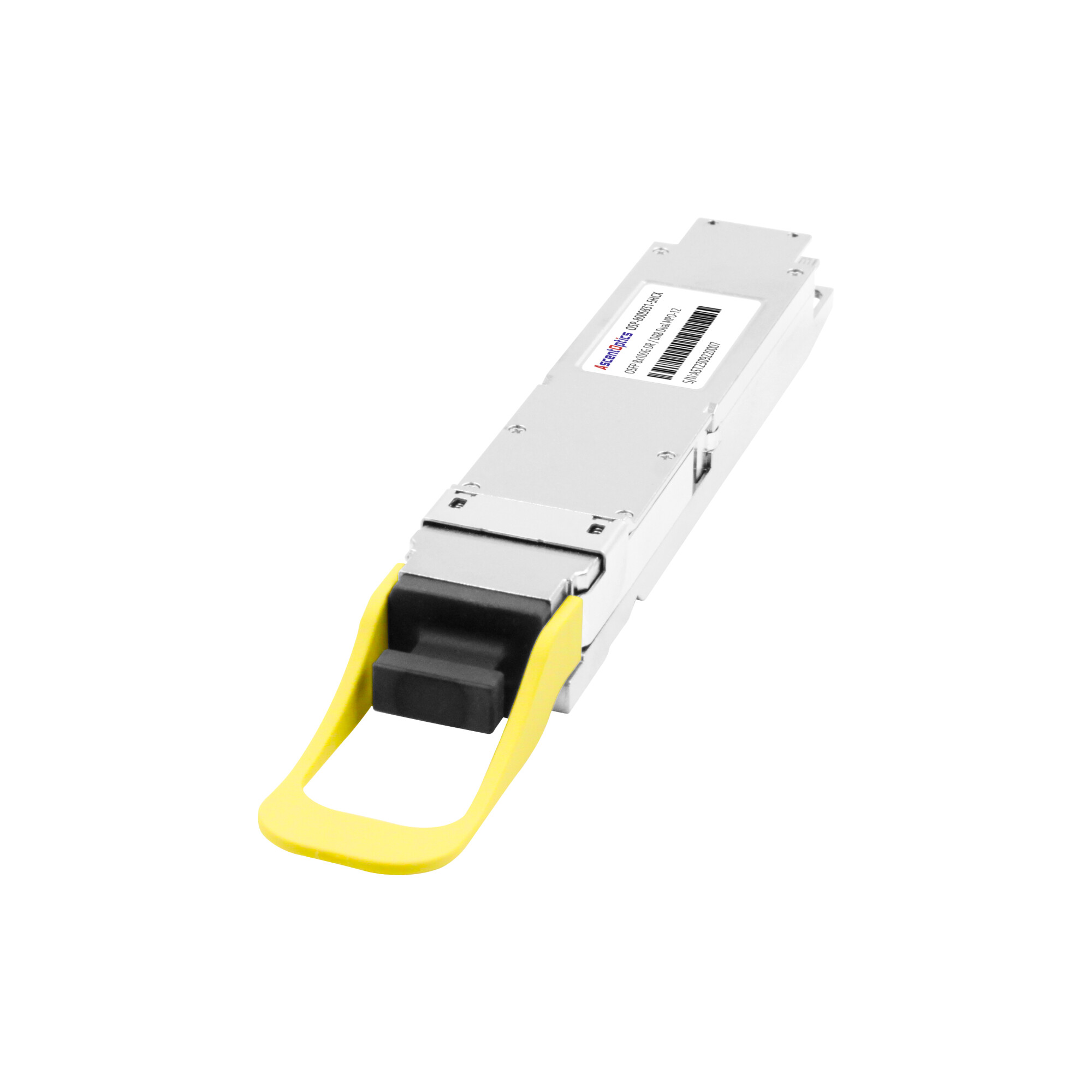
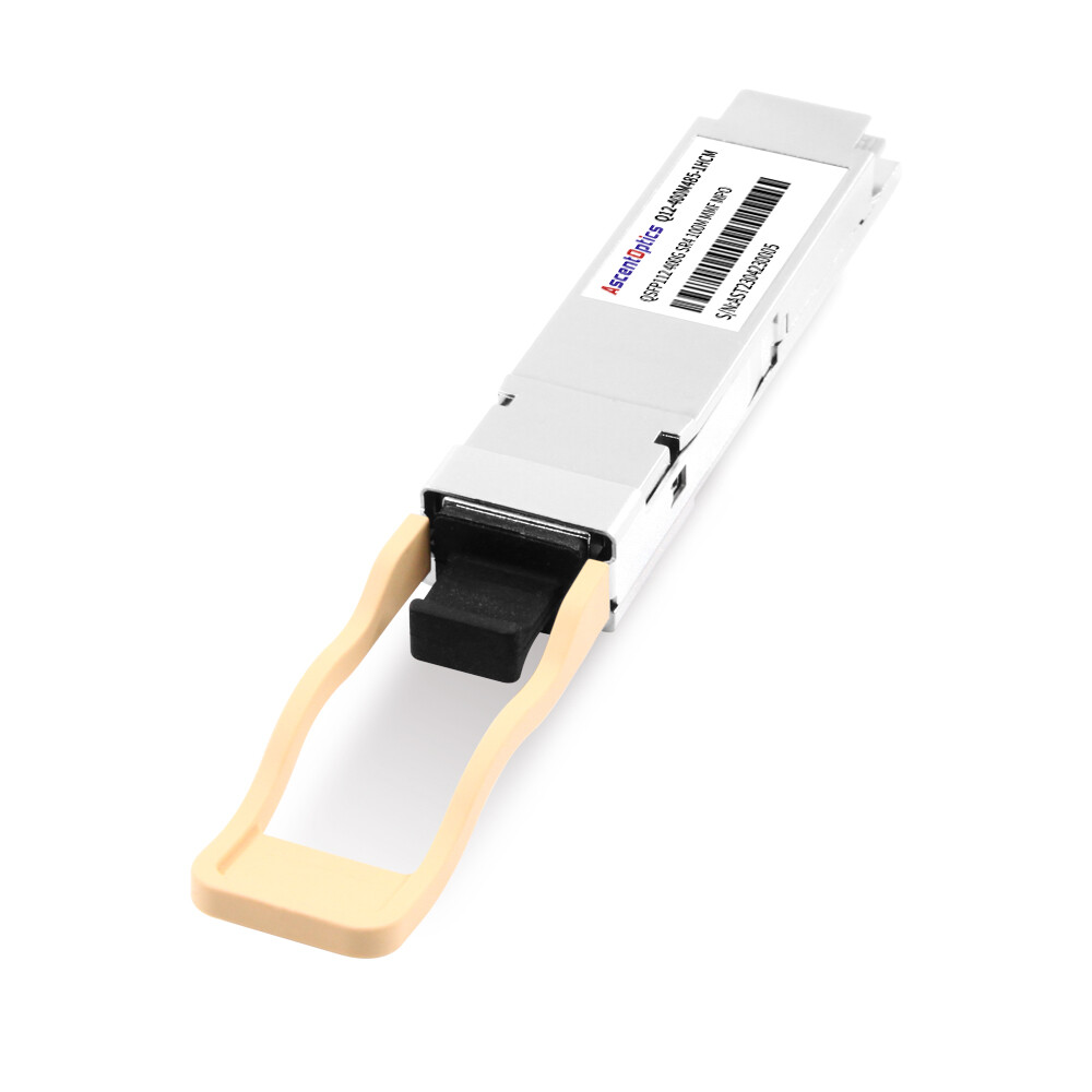
Bottlenecks of Traditional Architectures: In current data centers and high-performance computing (HPC), the speeds of computing units (CPU, GPU, ASIC) and network switch chips are increasing. They communicate via front-panel optical modules (such as OSFP, QSFP-DD) and optical fibers. The DSP (Digital Signal Processor) in the optical module is responsible for complex conversions and compensations between electrical and optical signals, but its power consumption increases dramatically with higher speeds.
Power Consumption Imbalance: At 1.6T (1.6Tbps) and higher speeds, the power consumption of a single optical module may reach over 20W. A high-end switch chip may require 32 or even 64 such ports, so the power consumption of the optical modules alone could reach hundreds of watts, even approaching or exceeding the power consumption of the switch chip itself. This greatly limits the overall performance and energy efficiency of the system, forming a “power wall”.
CPO Solution:
CPO integrates the optical engine (optical components) and electronic chips (switch chips or compute chiplets) within the same substrate or socket. This reduces the distance between them from the “meter level” (rack scale) to the “centimeter” or even “millimeter” level. Such ultra-short interconnect distances bring significant benefits:
Greatly reduced power consumption:
Shorter transmission distances mean minimal electrical signal attenuation and distortion, eliminating the need for high-power DSPs to perform complex signal compensation. Power consumption can be reduced by 30%–50%, which is critical for building green data centers and achieving higher computing performance.
2. Breaking Through the “Bandwidth Density” Limit
Physical Space Limitations: Front-panel optical modules require a large amount of physical space. As the number of ports and speeds increase, the front-panel area is no longer sufficient. There is an upper limit to the number of optical modules that can fit on the switch front panel.
CPO’s Solution: CPO moves the optical connections into the same package as the chip, shifting from two-dimensional (panel) wiring to three-dimensional (above the chip) stacking, greatly improving bandwidth density (the bandwidth that can be provided per unit area or volume). This enables a single switching device to support unprecedented total bandwidth, paving the way for future switch chips reaching 51.2T or even 102.4T.
3. Lowering Total Cost of Ownership (TCO)
Although the initial R&D and packaging costs of CPO are relatively high, it offers cost advantages from a system-wide perspective:
Fewer components: It eliminates the need for expensive housings, precision connectors, and long high-speed PCB traces on the motherboard (a very costly base material) used in traditional pluggable optical modules.
Simplified system design: Motherboard design becomes simpler, as there is no longer a need to route long, high-loss electrical traces for each port.
Reduced operational costs: The significant reduction in power consumption directly lowers electricity expenses and the cooling burden in data centers, leading to a substantial decrease in long-term operational costs (OpEx).
4. Enhancing Performance and Signal Integrity
Reduced electrical channel loss: Electrical signals experience severe loss and distortion when transmitted over long distances on PCBs. CPO shortens the electrical interconnect length to an extremely small scale, virtually eliminating such losses and enabling much higher data rates (e.g., future 224 Gbps per lane electrical I/O).
Improved integration: Silicon photonics technology allows large-scale manufacturing of optical devices (modulators, photodetectors, waveguides, etc.) on silicon wafers using mature CMOS processes. This enables tighter integration with electronic chips, resulting in better consistency and reliability.
Overall, as AI computing demands grow exponentially, traditional network architectures can no longer keep pace. As an innovative solution, CPO can greatly improve the efficiency, scalability, and sustainability of data centers, driving the industry toward higher efficiency.
Who Is Driving CPO? — Core Application Scenarios
Hyperscale data centers: Companies like Google, Meta, Amazon, and Microsoft are the main drivers. Their AI training clusters and intra–data center networks have insatiable demands for bandwidth and power efficiency.
AI / machine learning hardware: Companies such as NVIDIA, AMD, and Broadcom are adopting CPO technology in their next-generation GPUs and switching chips to overcome bandwidth bottlenecks in NVLink and InfiniBand.
High-performance computing (HPC): National supercomputing centers and research institutions need CPO to build exascale (10¹⁸ operations per second) and even more advanced supercomputers.
Conclusion
The development of CPO (co-packaged optics with silicon photonics) is not an optional path, but a necessary technological revolution in the post-Moore era to continuously enhance computing and networking performance and to cope with the exponentially growing data traffic and AI computing demands. By bringing optical interconnects as close as possible to the compute cores, CPO fundamentally addresses the three major bottlenecks of power consumption, bandwidth density, and signal integrity—making it a cornerstone technology for future high-performance computing and data center networks.
Post Views: 4,931